VTR CAD Flow
Fig. 1 illustrates the CAD flow typically used in VTR.
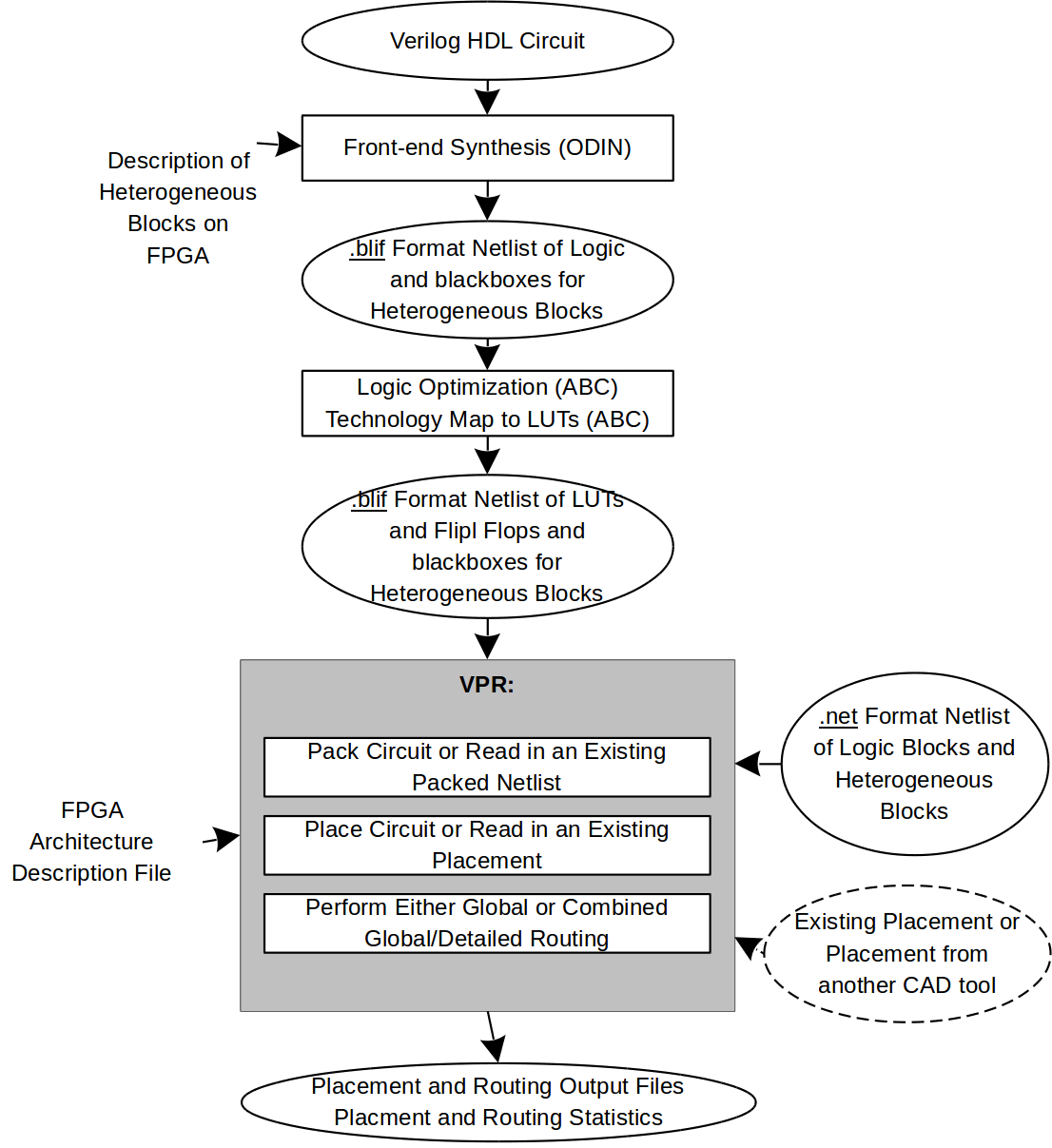
Fig. 1 Typicall VTR CAD Flow
First, Odin II converts a Verilog Hardware Destription Language (HDL) design into a flattened netlist consisting of logic gates and blackboxes that represent heterogeneous blocks [JKGS10].
Next, the ABC synthesis package is used to perform technology-independent logic optimization of each circuit, and then each circuit is technology-mapped into LUTs and flip flops [SG][PHMB07][CCMB07]. The output of ABC is a .blif format netlist of LUTs, flip flops, and blackboxes.
VPR then packs this netlist into more coarse-grained logic blocks, places the circuit, and routes it [BRM99][Bet98][BR96a][BR96b][BR97b][BR97a][MBR99][MBR00][BR00]. Generating output files for each stage. VPR will produce various statistics such as the minimum number of tracks per channel required to successfully route, the total wirelength, circuit speed, area and power.
Many variations on this CAD flow are possible. It is possible to use other high-level synthesis tools to generate the blif files that are passed into ABC. Also, one can use different logic optimizers and technology mappers than ABC; just put the output netlist from your technology-mapper into .blif format and feed it into VPR.
Alternatively, if the logic block you are interested in is not supported by VPR, your CAD flow can bypass VPR’s packer altogether by outputting a netlist of logic blocks in .net format. VPR can place and route netlists of any type of logic block – you simply have to create the netlist and describe the logic block in the FPGA architecture description file.
Finally, if you want only to route a placement produced by another CAD tool you can create a placement file in VPR format, and have VPR route this pre-existing placement.
VPR also supports timing analysis and power estimation.