VTR Quick Start
This is a quick introduction to VTR which covers how to run VTR and some of its associated tools (VPR, Parmys, ABC).
Setting Up VTR
Download VTR
The first step is to download VTR and extract it on your local machine.
Note
Developers planning to modify VTR should clone the VTR git repository.
Environment Setup
If you cloned the repository, you will need to set up the git submodules (if you downloaded and extracted a release, you can skip this step):
> git submodule init
> git submodule update
VTR requires several system and Python packages to build and run the flow. On Ubuntu and Debian systems, install the packages required by VTR using the command below.
Note
Developers planning to modify VTR should add the –dev option so extra packages for code formatting and functional verification are added.
> ./install_apt_packages.sh # add --dev if you plan to modify VTR code
Fedora and RHEL users instead use the command below to install the required system packages.
> ./install_dnf_packages.sh # add --dev if you plan to modify VTR code
Next install the required Python packages (optionally within a new Python virtual environment):
> make env                          # optional: install python virtual environment
> source .venv/bin/activate         # optional: activate python virtual environment
> pip install -r requirements.txt   # install python packages (in virtual environment if prior commands run, system wide otherwise)
Note
Developers who wish to modify VTR and are working on older Ubuntu versions (e.g. 20.04 or 22.04) must add clang-format-18 manually using the commands below. Note that this tool is only required if you want to run make format to automatically fix formatting issues in the code; it is not necessary for building or running VPR.
First add the LLVM APT repository to your system:
sudo apt install wget gnupg lsb-release
wget https://apt.llvm.org/llvm.sh
chmod +x llvm.sh
sudo ./llvm.sh 18
After that, you can install clang-format-18 using:
sudo apt install clang-format-18
Build VTR
On most unix-like systems you can run:
> make
Note
In the VTR documentation lines starting with > (like > make above), indicate a command (i.e. make) to run from your terminal.
When the \ symbol appears at the end of a line, it indicates line continuation.
Note
$VTR_ROOT refers to the root directory of the VTR project source tree. To run the examples in this guide on your machine, either:
define VTR_ROOT as a variable in your shell (e.g. if
~/trees/vtris the path to the VTR source tree on your machine, run the equivalent ofVTR_ROOT=~/trees/vtrin BASH) which will allow you to run the commands as written in this guide, ormanually replace $VTR_ROOT in the example commands below with your path to the VTR source tree.
For more details on building VTR on various operating systems/platforms see Building VTR.
Note
A plain make builds VPR headless (i.e. without graphics support — VPR runs place-and-route normally but cannot open a GUI window) unless a suitable Qt6 (>= 6.9.3) is present. To use the interactive GUI (--disp on, used in the visualization steps below) you must build VPR with graphics support — see VPR Graphics.
Running the VTR Flow
Running each stage of the flow manually is time consuming (and potentially error prone). For convenience, VTR provides a script (run_vtr_flow) which automates this process.
First, make sure you have activated the Python virtual environment created at the beginning of this tutorial:
> source $VTR_ROOT/.venv/bin/activate
Define the working directory where the flow will be executed. For convenience, use an environment variable:
export VTR_FLOW_DIR=~/vtr_work/quickstart/blink_run_flow
Alternatively, you can manually replace $VTR_FLOW_DIR with your preferred directory path in the commands below.
Create the working directory and navigate into it:
> mkdir -p $VTR_FLOW_DIR
> cd $VTR_FLOW_DIR
Now lets run the script ($VTR_ROOT/vtr_flow/scripts/run_vtr_flow.py) passing in:
The circuit verilog file (
$VTR_ROOT/doc/src/quickstart/blink.v)The FPGA architecture file (
$VTR_ROOT/vtr_flow/arch/timing/EArch.xml)
and also specifying the options:
--route_chan_width 100a fixed FPGA routing architecture channel width.
The resulting command is:
> $VTR_ROOT/vtr_flow/scripts/run_vtr_flow.py \
    $VTR_ROOT/doc/src/quickstart/blink.v \
    $VTR_ROOT/vtr_flow/arch/timing/EArch.xml \
    --route_chan_width 100
Note
Options unrecognized by run_vtr_flow (like --route_chan_width) are passed on to VPR.
which should produce output similar to:
EArch/blink OK (took 0.26 seconds, overall memory peak 63.71 MiB consumed by vpr run)
There are also multiple log files (including for ABC, Parmys and VPR), which by convention the script names with the .out suffix:
> ls $VTR_FLOW_DIR/temp/*.out

0_blackboxing_latch.out  parmys.out        report_clocks.abc.out  vanilla_restore_clocks.out
abc0.out                 report_clk.out  restore_latch0.out     vpr.out
With the main log files of interest including the Parmys log file (parmys.out), log files produced by ABC (e.g. abc0.out), and the VPR log file (vpr.out).
Note
ABC may be invoked multiple times if a circuit has multiple clock domains, producing multiple log files (abc0.out, abc1.out, …)
You will also see there are several BLIF files produced:
> ls $VTR_FLOW_DIR/temp/*.blif

0_blink.abc.blif   0_blink.raw.abc.blif  blink.parmys.blif
0_blink.parmys.blif  blink.abc.blif        blink.pre-vpr.blif
With the main files of interest being blink.parmys.blif (netlist produced by Parmys), blink.abc.blif (final netlist produced by ABC after clock restoration), blink.pre-vpr.blif netlist used by VPR (usually identical to blink.abc.blif).
Like before, we can also see the implementation files generated by VPR:
> ls $VTR_FLOW_DIR/temp/*.net $VTR_FLOW_DIR/temp/*.place $VTR_FLOW_DIR/temp/*.route

blink.net  blink.place  blink.route
which we can visualize with:
> cd $VTR_FLOW_DIR/temp
> $VTR_ROOT/vpr/vpr \
    $VTR_ROOT/vtr_flow/arch/timing/EArch.xml \
    blink --circuit_file $VTR_FLOW_DIR/temp/blink.pre-vpr.blif \
    --route_chan_width 100 \
    --analysis --disp on
Note
When --analysis is provided, the VPR flow will attempt to read the prior optimization output files (.net, .place and .route) under temp, and hence we need to cd to that directory. If it is not provided, this step is optional.
Running VPR Manually
Sometimes you may wish to run only the vpr (placement, routing and timing analysis) parts of the flow rather than the full VTR flow (which includes synthesis). To show how to do this, let’s now try taking a simple pre-synthesized circuit (consisting of LUTs and Flip-Flops) and use the VPR tool to implement it on a specific FPGA architecture.
Running VPR on a Pre-Synthesized Circuit
First, let’s make a directory in our home directory where we can work:
#Move to our home directory
> cd ~

#Make a working directory
> mkdir -p vtr_work/quickstart/vpr_tseng

#Move into the working directory
> cd ~/vtr_work/quickstart/vpr_tseng
Now, lets invoke the VPR tool to implement:
the
tsengcircuit ($VTR_ROOT/vtr_flow/benchmarks/blif/tseng.blif), onthe
EArchFPGA architecture ($VTR_ROOT/vtr_flow/arch/timing/EArch.xml).
We do this by passing these files to the VPR tool, and also specifying that we want to route the circuit on a version of EArch with a routing architecture channel width of 100 (--route_chan_width 100):
> $VTR_ROOT/vpr/vpr \
    $VTR_ROOT/vtr_flow/arch/timing/EArch.xml \
    $VTR_ROOT/vtr_flow/benchmarks/blif/tseng.blif \
    --route_chan_width 100
This will produce a large amount of output as VPR implements the circuit, but you should see something similar to:
VPR FPGA Placement and Routing.
Version: 8.1.0-dev+2b5807ecf
Revision: v8.0.0-1821-g2b5807ecf
Compiled: 2020-05-21T16:39:33
Compiler: GNU 7.3.0 on Linux-4.15.0-20-generic x86_64
Build Info: release VTR_ASSERT_LEVEL=2

University of Toronto
verilogtorouting.org
vtr-users@googlegroups.com
This is free open source code under MIT license.

#
#Lots of output trimmed for brevity....
#

Geometric mean non-virtual intra-domain period: 6.22409 ns (160.666 MHz)
Fanout-weighted geomean non-virtual intra-domain period: 6.22409 ns (160.666 MHz)

VPR succeeded
The entire flow of VPR took 3.37 seconds (max_rss 40.7 MiB)
which shows that VPR as successful (VPR succeeded), along with how long VPR took to run (~3 seconds in this case).
You will also see various result files generated by VPR which define the circuit implementation:
> ls *.net *.place *.route

tseng.net  tseng.place  tseng.route
along with a VPR log file which contains what VPR printed when last invoked:
> ls *.log

vpr_stdout.log
and various report files describing the characteristics of the implementation:
> ls *.rpt

packing_pin_util.rpt              report_timing.hold.rpt   report_unconstrained_timing.hold.rpt
pre_pack.report_timing.setup.rpt  report_timing.setup.rpt  report_unconstrained_timing.setup.rpt
Visualizing Circuit Implementation
Note
This section requires that VPR was compiled with graphic support. See VPR Graphics for details.
The .net, .place and .route files (along with the input .blif and architecture .xml files) fully defined the circuit implementation.
We can visualize the circuit implementation by:
Re-running VPR’s analysis stage (
--analysis), andenabling VPR’s graphical user interface (
--dispon).
This is done by running the following:
> $VTR_ROOT/vpr/vpr \
    $VTR_ROOT/vtr_flow/arch/timing/EArch.xml \
    $VTR_ROOT/vtr_flow/benchmarks/blif/tseng.blif \
    --route_chan_width 100 \
    --analysis --disp on
which should open the VPR graphics and allow you to explore the circuit implementation.
As an exercise try the following:
View the connectivity of a block (connections which drive it, and those which it drives)
View the internals of a logic block (e.g. try to find the LUTs/
.namesand Flip-Flops/.latch)Visualize all the routed circuit connections
See also
For more details on the various graphics options, see VPR Graphics
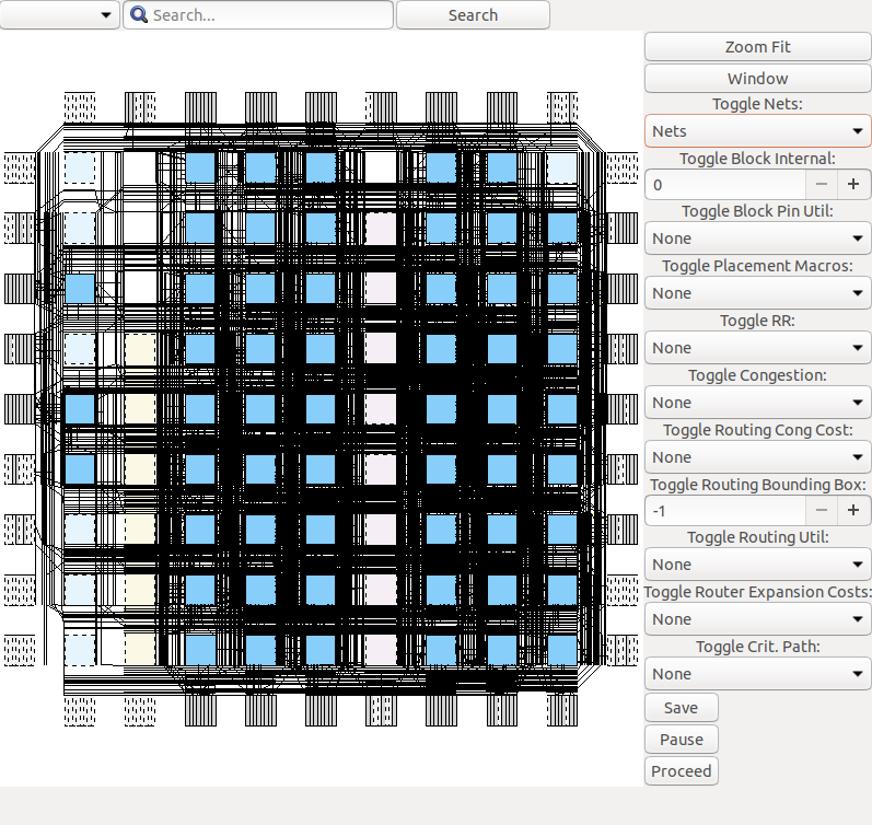
Fig. 1 Routed net connections of tseng on EArch.
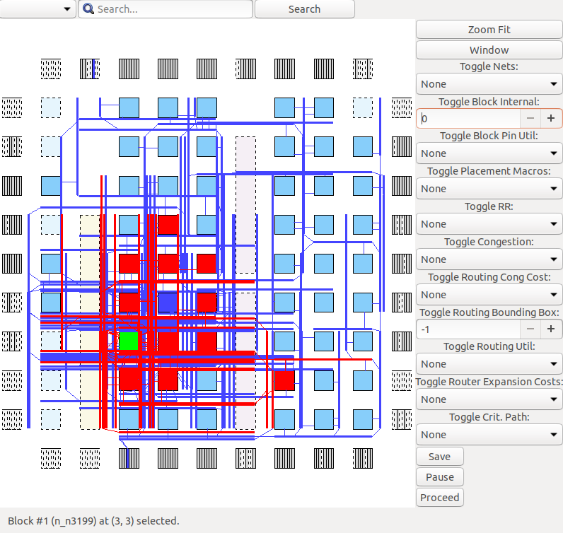
Fig. 2 Input (blue)/output (red) nets of block n_n3226 (highlighted green).
Note
If you do not provide --analysis, VPR will re-implement the circuit from scratch.
If you also specify --disp on, you can see how VPR modifies the implementation as it runs.
By default --disp on stops at key stages to allow you to view and explore the implementation.
You will need to press the Proceed button in the GUI to allow VPR to continue to the next stage.
Manually Running the VTR Flow
In the previous section we have implemented a pre-synthesized circuit onto a pre-existing FPGA architecture using VPR, and visualized the result. We now turn to how we can implement our own circuit on a pre-existing FPGA architecture.
To do this, we begin by describing a circuit behaviourally using the Verilog Hardware Description Language (HDL). This allows us to quickly and consisely define the circuit’s behaviour. We will then use the VTR Flow to synthesize the behavioural Verilog description into a circuit netlist, and implement it onto an FPGA.
Example Circuit
We will use the following simple example circuit, which causes its output to toggle on and off:
 1//A simple cricuit which blinks an LED on and off periodically
 2module blink(
 3    input clk,      //Input clock
 4    input i_reset,  //Input active-high reset
 5    output o_led);  //Output to LED
 6
 7    //Sequential logic
 8    //
 9    //A reset-able counter which increments each clock cycle
10    reg[4:0] r_counter;
11    always @(posedge clk) begin
12        if (i_reset) begin //When reset is high, clear counter
13            r_counter <= 5'd0;
14        end else begin //Otherwise increment counter each clock (note that it will overflow back to zero)
15            r_counter <= r_counter + 1'b1;
16        end
17    end
18
19    //Combinational logic
20    //
21    //Drives o_led high if count is below a threshold
22    always @(*) begin
23        if (r_counter < 5'd16) begin
24            o_led <= 1'b1;
25        end else begin
26            o_led <= 1'b0;
27        end
28    end
29
30endmodule
This Verilog creates a sequential 5-bit register (r_counter) which increments every clock cycle.
If the count is below 16 it drives the output (o_led) high, otherwise it drives it low.
With the circuit defined, we are now ready to move forward with implementing it on an FPGA. To begin the process, we’ll set up a fresh working directory where we can manage our files and run the necessary VTR flow steps. Let’s get started by creating that directory and organizing our workspace:
$WRK_DIRwill serve as our working directory for this example.
To set this variable, define it in your shell:
export WRK_DIR=~/vtr_work/quickstart/blink_manual
Alternatively, manually replace $WRK_DIR in the example commands with your path.
Now, create and navigate to the working directory:
> mkdir -p $WRK_DIR
> cd $WRK_DIR
Next, we need to run the three main sets of tools, depending on the method of synthesis you choose:
Synthesis Options:
Parmys: Parmys is the default synthesis tool in the VTR flow.
Odin II: Odin II is the alternative synthesis tool supported by VTR.
Finally, regardless of the synthesis method, run ABC to perform logic optimization and technology mapping, and then run VPR to handle packing, placement, and routing, which completes the implementation on the FPGA architecture.
Synthesizing with Parmys
To synthesize our Verilog file into a circuit netlist, we will utilize the run_vtr_flow.py script, which streamlines the process. This command synthesizes the provided Verilog file (blink.v) while targeting the specified FPGA architecture (EArch.xml).
The command is as follows:
> $VTR_ROOT/vtr_flow/scripts/run_vtr_flow.py \
    $VTR_ROOT/doc/src/quickstart/blink.v \
    $VTR_ROOT/vtr_flow/arch/timing/EArch.xml \
    -start parmys -end parmys
When executed, the output should indicate successful synthesis, similar to:
EArch/blink OK (took 0.16 seconds, overall memory peak 20.00 MiB consumed by parmys run)
This output confirms that the synthesis was successful and provides information on the duration and memory usage during the process.
We can now take a look at the circuit which Parmys produced (blink.parmys.blif).
See also
For more information on the BLIF file format see BLIF Netlist (.blif).
Optimizing and Technology Mapping with ABC
Next, we’ll optimize and technology map our circuit using ABC, providing the option:
-c <script>, where<script>is a set of commands telling ABC how to synthesize our circuit.
We’ll use the following, simple ABC commands:
read blink.parmys.blif;                               #Read the circuit synthesized by parmys
if -K 6;                                            #Technology map to 6 input LUTs (6-LUTs)
write_hie blink.parmys.blif blink.abc_no_clock.blif   #Write new circuit to blink.abc_no_clock.blif
Note
Usually you should use a more complicated script (such as that used by run_vtr_flow) to ensure ABC optimizes your circuit well.
The corresponding command to run is:
> $VTR_ROOT/abc/abc \
    -c "read $WRK_DIR/temp/blink.parmys.blif; if -K 6; write_hie $WRK_DIR/temp/blink.parmys.blif $WRK_DIR/temp/blink.abc_no_clock.blif"
When run, ABC’s output should look similar to:
ABC command line: "read blink.parmys.blif; if -K 6; write_hie blink.parmys.blif blink.abc_no_clock.blif".

Hierarchy reader converted 6 instances of blackboxes.
The network was strashed and balanced before FPGA mapping.
Hierarchy writer reintroduced 6 instances of blackboxes.
If we now inspect the produced BLIF file (blink.abc_no_clock.blif) we see that ABC was able to significantly simplify and optimize the circuit’s logic (compared to blink.parmys.blif):
 1# Benchmark "blink" written by ABC on Tue May 19 15:42:50 2020
 2.model blink
 3.inputs blink^clk blink^i_reset
 4.outputs blink^o_led
 5
 6.latch        n19 blink^r_counter~0_FF  2
 7.latch        n24 blink^r_counter~4_FF  2
 8.latch        n29 blink^r_counter~3_FF  2
 9.latch        n34 blink^r_counter~2_FF  2
10.latch        n39 blink^r_counter~1_FF  2
11
12
13.subckt adder a[0]=blink^r_counter~0_FF b[0]=vcc cin[0]=blink^ADD~2-0[0] cout[0]=blink^ADD~2-1[0] sumout[0]=blink^ADD~2-1[1]
14.subckt adder a[0]=blink^r_counter~1_FF b[0]=gnd cin[0]=blink^ADD~2-1[0] cout[0]=blink^ADD~2-2[0] sumout[0]=blink^ADD~2-2[1]
15.subckt adder a[0]=blink^r_counter~2_FF b[0]=gnd cin[0]=blink^ADD~2-2[0] cout[0]=blink^ADD~2-3[0] sumout[0]=blink^ADD~2-3[1]
16.subckt adder a[0]=blink^r_counter~3_FF b[0]=gnd cin[0]=blink^ADD~2-3[0] cout[0]=blink^ADD~2-4[0] sumout[0]=blink^ADD~2-4[1]
17.subckt adder a[0]=blink^r_counter~4_FF b[0]=gnd cin[0]=blink^ADD~2-4[0] cout[0]=blink^ADD~2-5[0] sumout[0]=blink^ADD~2-5[1]
18.subckt adder a[0]=gnd b[0]=gnd cin[0]=unconn cout[0]=blink^ADD~2-0[0] sumout[0]=blink^ADD~2-0~dummy_output~0~1
19
20
21.names blink^i_reset blink^ADD~2-1[1] n19
2201 1
23.names blink^i_reset blink^ADD~2-5[1] n24
2401 1
25.names blink^i_reset blink^ADD~2-4[1] n29
2601 1
27.names blink^i_reset blink^ADD~2-3[1] n34
2801 1
29.names blink^i_reset blink^ADD~2-2[1] n39
3001 1
31.names vcc
32 1
33.names gnd
34 0
35.names unconn
36 0
37.names blink^r_counter~4_FF blink^o_led
380 1
39.end
40
41
42.model adder
43.inputs a[0] b[0] cin[0]
44.outputs cout[0] sumout[0]
45.blackbox
46.end
ABC has kept the .latch and .subckt adder primitives, but has significantly simplified the other logic (.names).
However, there is an issue with the above BLIF produced by ABC: the latches (rising edge Flip-Flops) do not have any clocks or edge sensitivity specified, which is information required by VPR.
Re-inserting clocks
We will restore the clock information by running a script which will transfer that information from the original parmys BLIF file (writing it to the new file blink.pre-vpr.blif):
> $VTR_ROOT/vtr_flow/scripts/restore_multiclock_latch.pl \
    $WRK_DIR/temp/blink.parmys.blif \
    $WRK_DIR/temp/blink.abc_no_clock.blif \
    $WRK_DIR/temp/blink.pre-vpr.blif
If we inspect blink.pre-vpr.blif we now see that the clock (blink^clk) has been restored to the Flip-Flops:
> grep 'latch' blink.pre-vpr.blif

.latch n19 blink^r_counter~0_FF re blink^clk 3
.latch n24 blink^r_counter~4_FF re blink^clk 3
.latch n29 blink^r_counter~3_FF re blink^clk 3
.latch n34 blink^r_counter~2_FF re blink^clk 3
.latch n39 blink^r_counter~1_FF re blink^clk 3
Implementing the circuit with VPR
Now that we have the optimized and technology mapped netlist (blink.pre-vpr.blif), we can invoke VPR to implement it onto the EArch FPGA architecture (in the same way we did with the tseng design earlier).
However, since our BLIF file doesn’t match the design name we explicitly specify:
blinkas the circuit name, andthe input circuit file with
--circuit_file.
to ensure the resulting .net, .place and .route files will have the correct names.
The resulting command is:
> $VTR_ROOT/vpr/vpr \
    $VTR_ROOT/vtr_flow/arch/timing/EArch.xml \
    blink --circuit_file $WRK_DIR/temp/blink.pre-vpr.blif \
    --route_chan_width 100
and after VPR finishes we should see the resulting implementation files:
> ls $WRK_DIR/*.net $WRK_DIR/*.place $WRK_DIR/*.route

blink.net  blink.place  blink.route
We can then view the implementation as usual by appending --analysis --disp on to the command:
> $VTR_ROOT/vpr/vpr \
    $VTR_ROOT/vtr_flow/arch/timing/EArch.xml \
    blink --circuit_file $WRK_DIR/temp/blink.pre-vpr.blif \
    --route_chan_width 100 \
    --analysis --disp on
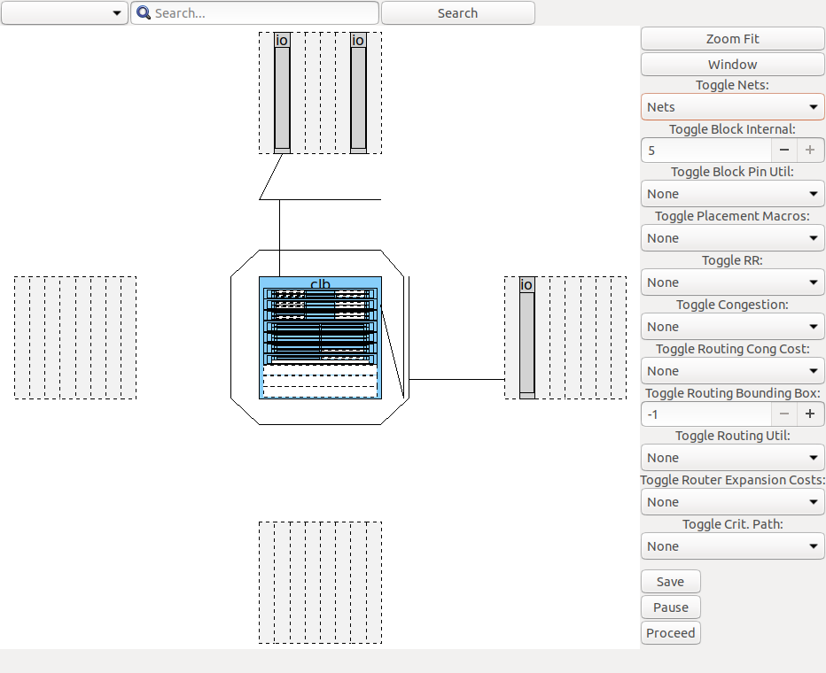
Fig. 3 blink.v circuit implementation on the EArch FPGA architecture as viewed in the VPR GUI
Manually Running VTR with ODIN II
VTR includes a second synthesis tool, ODIN II. Below we explain how to run this alternative synthesis flow.
To synthesize your Verilog design with ODIN II, you need to build VTR with the following command:
> cd ~/$VTR_ROOT
> make CMAKE_PARAMS="-DWITH_ODIN=on"
This step enables ODIN II support in the VTR build process, which is essential for the subsequent synthesis operations.
Lets make a new directory for us to work in:
> mkdir -p ~/vtr_work/quickstart/blink_manual
> cd ~/vtr_work/quickstart/blink_manual
Next, run ODIN II on your Verilog file to synthesize it into a circuit netlist. Use the command below, specifying the required options:
-a $VTR_ROOT/vtr_flow/arch/timing/EArch.xmlwhich specifies what FPGA architecture we are targeting,
-V $VTR_ROOT/doc/src/quickstart/blink.vwhich specifies the verilog file we want to synthesize, and
-o blink.odin.blifwhich specifies the name of the generated.blifcircuit netlist.
The resulting command is:
> $VTR_ROOT/odin_ii/odin_ii \
    -a $VTR_ROOT/vtr_flow/arch/timing/EArch.xml \
    -V $VTR_ROOT/doc/src/quickstart/blink.v \
    -o blink.odin.blif
After running the command, you should see an output similar to the following:
Total time: 14.7ms
Odin ran with exit status: 0
Odin II took 0.01 seconds (max_rss 5.1 MiB)
where Odin ran with exit status: 0 indicates Odin successfully synthesized our verilog.
We can now take a look at the circuit which ODIN produced (blink.odin.blif).
The file is long and likely harder to follow than our code in blink.v; however it implements the same functionality.
Some interesting highlights are shown below:
blink.odin.blif (implements part of r_counter in blink.v).latch blink^nMUX~0^MUX_2~23 blink^r_counter~0_FF re blink^clk 3
.latch blink^nMUX~0^MUX_2~27 blink^r_counter~4_FF re blink^clk 3
blink.odin.blif, used to perform addition (implements part of the + operator in blink.v).subckt adder a[0]=blink^r_counter~0_FF b[0]=vcc cin[0]=blink^ADD~2-0[0]\
cout[0]=blink^ADD~2-1[0] sumout[0]=blink^ADD~2-1[1]
.subckt adder a[0]=blink^r_counter~1_FF b[0]=gnd cin[0]=blink^ADD~2-1[0]\
cout[0]=blink^ADD~2-2[0] sumout[0]=blink^ADD~2-2[1]
blink.odin.blif, implementing logical OR (implements part of the < operator in blink.v).names blink^LT~4^GT~10 blink^LT~4^GT~12 blink^LT~4^GT~14 blink^LT~4^GT~16 blink^LT~4^GT~18 blink^LT~4^lOR~9
1---- 1
-1--- 1
--1-- 1
---1- 1
----1 1
See also
For more information on the BLIF file format see BLIF Netlist (.blif).
After generating blink.odin.blif, we can proceed to optimize the netlist and implement it on the FPGA. Follow the steps outlined in the section titled Optimizing and Technology Mapping with ABC, using the generated blink.odin.blif as input instead of blink.parmys.blif.
Once the netlist is optimized with ABC, continue with the Implementing the circuit with VPR section to pack, place, and route the circuit onto the FPGA architecture.
Next Steps
Now that you’ve finished the VTR quickstart, you’re ready to start experimenting and using VTR.
Here are some possible next steps for users wishing to use VTR:
Try modifying the Verilog file (e.g.
blink.v) or make your own circuit and try running it through the flow.Learn about FPGA architecture modelling (Tutorials, Reference), and try modifying a copy of
EArchto see how it changes the implementation ofblink.v.Read more about the VTR CAD Flow, and Task automation framework.
Find out more about using other benchmark sets, like how to run the Titan Benchmark Suite.
Discover how to generate FASM for bitstream creation.
Here are some possible next steps for developers wishing to modify and improve VTR:
Try the next steps listed for users above to learn how VTR is used.
Work through the new developer tutorial.
Read through the developer guide.
Look for open issues to which you can contribute.
Begin exploring the source code for the main tools in VTR (e.g. VPR in
$VTR_ROOT/vpr/src).