Architecture Reference
This section provides a detailed reference for the FPGA Architecture description used by VTR. The Architecture description uses XML as its representation format.
As a convention, curly brackets { } represents an option with each option separated by |. For example, a={1 | 2 | open} means field a can take a value of 1, 2, or open.
Recognized BLIF Models (<models>)
The <models> tag contains <model name="string" never_prune="string"> tags.
Each <model> tag describes the BLIF .subckt model names that are accepted by the FPGA architecture.
The name of the model must match the corresponding name of the BLIF model.
The never_prune flag is optional and can be either:
false (default)
true
Normally blocks with no output nets are pruned away by the netlist sweepers in vpr (removed from the netlist); this is the default behaviour. If never_prune = “true” is set on a model, then blocks that are instances of that model will not be swept away during netlist cleanup. This can be helpful for some special blocks that do have only input nets and are required to be placed on the device for some features to be active, so space on the chip is still reserved for them, despite them not driving any connection. One example is the IDELAYCTRL of the Series7 devices, which takes as input a reference clock and internally controls and synchronizes all the IDELAYs in a specific clock region, with no output net necessary for it to function correctly.
Note
Standard blif structures (.names, .latch, .input, .output) are accepted by default, so these models should not be described in the <models> tag.
Each model tag must contain 2 tags: <input_ports> and <output_ports>.
Each of these contains <port> tags:
- <port name="string" is_clock="{0 | 1} clock="string" combinational_sink_ports="string1 string2 ..."/>" title="Link to this definition">
- Required Attributes:
name – The port name.
- Optional Attributes:
is_clock –
Identifies if the port is a clock port.
See also
The Primitive Timing Modelling Tutorial for usage of
is_clockto model clock control blocks such as clock generators, clock buffers/gates and clock muxes.Default:
0clock – Indicates the port is sequential and controlled by the specified clock (which must be another port on the model marked with
is_clock=1). Default: port is treated as combinational (if unspecified)combinational_sink_ports – A space-separated list of output ports which are combinationally connected to the current input port. Default: No combinational connections (if unspecified)
Defines the port for a model.
An example models section containing a combinational primitive adder and a sequential primitive single_port_ram follows:
<models>
  <model name="single_port_ram">
    <input_ports>
      <port name="we" clock="clk" />
      <port name="addr" clock="clk" combinational_sink_ports="out"/>
      <port name="data" clock="clk" combinational_sink_ports="out"/>
      <port name="clk" is_clock="1"/>
    </input_ports>
    <output_ports>
      <port name="out" clock="clk"/>
    </output_ports>
  </model>

  <model name="adder">
    <input_ports>
      <port name="a" combinational_sink_ports="cout sumout"/>
      <port name="b" combinational_sink_ports="cout sumout"/>
      <port name="cin" combinational_sink_ports="cout sumout"/>
    </input_ports>
    <output_ports>
      <port name="cout"/>
      <port name="sumout"/>
    </output_ports>
  </model>
</models>
Note that for single_port_ram above, the ports we, addr, data, and out are sequential since they have a clock specified.
Additionally addr and data are shown to be combinationally connected to out; this corresponds to an internal timing path between the addr and data input registers, and the out output registers.
For the adder the input ports a, b and cin are each combinationally connected to the output ports cout and sumout (the adder is a purely combinational primitive).
See also
For more examples of primitive timing modeling specifications see the Primitive Block Timing Modeling Tutorial
Global FPGA Information
- <tiles>content</tiles>
Content inside this tag contains a group of
<pb_type>tags that specify the types of functional blocks and their properties.
- <layout/>
Content inside this tag specifies device grid layout.
See also
- <layer die='int'>content</layer>
Content inside this tag specifies the layout of a single (2D) die; using multiple layer tags one can describe multi-die FPGAs (e.g. 3D stacked FPGAs).
- <device>content</device>
Content inside this tag specifies device information.
See also
- <switchlist>content</switchlist>
Content inside this tag contains a group of <switch> tags that specify the types of switches and their properties.
- <segmentlist>content</segmentlist>
Content inside this tag contains a group of <segment> tags that specify the types of wire segments and their properties.
- <complexblocklist>content</complexblocklist>
Content inside this tag contains a group of
<pb_type>tags that specify the types of functional blocks and their properties.
- <noc link_bandwidth="float" link_latency="float" router_latency="float" noc_router_tile_name="string">content</noc>content" title="Link to this definition">
Content inside this tag specifies the Network-on-Chip (NoC) architecture on the FPGA device and its properties.
FPGA Grid Layout
The valid tags within the <layout> tag are:
- <auto_layout aspect_ratio="float">" title="Link to this definition">
- Optional Attributes:
aspect_ratio –
The device grid’s target aspect ratio (
 )
)Default:
1.0
Defines a scalable device grid layout which can be automatically scaled to a desired size.
Note
At most one
<auto_layout>can be specified.
- <fixed_layout name="string" width="int" height="int">" title="Link to this definition">
- Required Attributes:
name – The unique name identifying this device grid layout.
width – The device grid width
height – The device grid height
Defines a device grid layout with fixed dimensions.
Note
Multiple
<fixed_layout>tags can be specified.
Each <auto_layout> or <fixed_layout> tag should contain a set of grid location tags.
FPGA Layer Information
The layer tag is an optional tag to specify multi-die FPGAs. If not specified, a single-die FPGA with a single die (with index 0) is assumed.
- <layer die="int">" title="Link to this definition">
- Optional Attributes:
die –
Specifies the index of the die; index 0 is assumed to be at the bottom of a stack.
Default:
0
Note
If die number left unspecified, a single-die FPGA (die number = 0) is assumed.
<!-- Describe 3D FPGA using layer tag -->
<fixed_layout name="3D-FPGA" width="device_width" height="device_height">
    <!-- First die (base die) -->
    <layer die="0"/>
        <!-- Specify base die Grid layout (e.g., fill with Network-on-Chips) -->
        <fill type="NoC">
    </layer>
    <!-- Second die (upper die) -->
    <layer die="1">
        <!-- Specify upper die Grid layout (e.g., fill with logic blocks) -->
        <fill type="LAB">
    </layer>
</fixed_layout>
Note
Note that all dice have the same width and height. Since we can always fill unused parts of a die with EMPTY blocks this does not restrict us to have the same usable area on each die.
Grid Location Priorities
Each grid location specification has an associated numeric priority. Larger priority location specifications override those with lower priority.
Note
If a grid block is partially overlapped by another block with higher priority the entire lower priority block is removed from the grid.
Empty Grid Locations
Empty grid locations can be specified using the special block type EMPTY.
Note
All grid locations default to EMPTY unless otherwise specified.
TSV Hole Grid Locations
In multi-die devices, through-silicon via (TSV) holes reserved for power delivery occupy silicon area and prevent inter-layer connectivity at those grid locations. These regions are modeled as ordinary tiles (with any name) placed in the device layout at the corresponding grid locations.
The tile should use pattern="custom" in <switchblock_locations> with <sb_loc type="straight_short"> entries at each switchblock location.
This electrically shorts routing wires straight-through using same-track (ptc) connections.
The tile should typically also set Fc = 0 so that no block-pin routing connections are created.
VPR skips inter-layer scatter-gather links when either the gather or scatter endpoint has a short switchblock type (horizontal_short, vertical_short, or straight_short).
Example of a TSV hole tile:
<tile name="tsv_hole" height="2" width="2" area="0">
    <switchblock_locations pattern="custom">
        <sb_loc type="straight_short" xoffset="0" yoffset="0"/>
        <sb_loc type="straight_short" xoffset="0" yoffset="1"/>
        <sb_loc type="straight_short" xoffset="1" yoffset="0"/>
        <sb_loc type="straight_short" xoffset="1" yoffset="1"/>
    </switchblock_locations>
    <sub_tile name="tsv_hole">
        <equivalent_sites>
            <site pb_type="tsv_hole"/>
        </equivalent_sites>
        <input name="I" num_pins="1"/>
        <output name="O" num_pins="1"/>
        <fc in_type="abs" in_val="0" out_type="abs" out_val="0"/>
    </sub_tile>
</tile>
Grid Location Expressions
Some grid location tags have attributes (e.g. startx) which take an expression as their argument.
An expression can be an integer constant, or simple mathematical formula evaluated when constructing the device grid.
Supported operators include: +, -, *, /, along with ( and ) to override the default evaluation order.
Expressions may contain numeric constants (e.g. 7) and the following special variables:
W: The width of the deviceH: The height of the devicew: The width of the current block typeh: The height of the current block type
Warning
All expressions are evaluated as integers, so operations such as division may have their result truncated.
As an example consider the expression W/2 - w/2.
For a device width of 10 and a block type of width 3, this would be evaluated as  .
.
Grid Location Tags
- <fill type="string" priority="int"/>" title="Link to this definition">
- Required Attributes:
type – The name of the top-level complex block type (i.e.
<pb_type>) being specified.priority – The priority of this layout specification. Tags with higher priority override those with lower priority.
Fills the device grid with the specified block type.
Example:
<!-- Fill the device with CLB blocks -->
<fill type="CLB" priority="1"/>

Fig. 14 <fill> CLB example
- <perimeter type="string" priority="int"/>" title="Link to this definition">
- Required Attributes:
type – The name of the top-level complex block type (i.e.
<pb_type>) being specified.priority – The priority of this layout specification. Tags with higher priority override those with lower priority.
Sets the perimeter of the device (i.e. edges) to the specified block type.
Note
The perimeter includes the corners
Example:
<!-- Create io blocks around the device perimeter -->
<perimeter type="io" priority="10"/>

Fig. 15 <perimeter> io example
- <corners type="string" priority="int"/>" title="Link to this definition">
- Required Attributes:
type – The name of the top-level complex block type (i.e.
<pb_type>) being specified.priority – The priority of this layout specification. Tags with higher priority override those with lower priority.
Sets the corners of the device to the specified block type.
Example:
<!-- Create PLL blocks at all corners -->
<corners type="PLL" priority="20"/>

Fig. 16 <corners> PLL example
- <single type="string" priority="int" x="expr" y="expr"/>" title="Link to this definition">
- Required Attributes:
type – The name of the top-level complex block type (i.e.
<pb_type>) being specified.priority – The priority of this layout specification. Tags with higher priority override those with lower priority.
x – The horizontal position of the block type instance.
y – The vertical position of the block type instance.
Specifies a single instance of the block type at a single grid location.
Example:
<!-- Create a single instance of a PCIE block (width 3, height 5)
     at location (1,1)-->
<single type="PCIE" x="1" y="1" priority="20"/>

Fig. 17 <single> PCIE example
- <col type="string" priority="int" startx="expr" repeatx="expr" starty="expr" incry="expr"/>" title="Link to this definition">
- Required Attributes:
type – The name of the top-level complex block type (i.e.
<pb_type>) being specified.priority – The priority of this layout specification. Tags with higher priority override those with lower priority.
startx – An expression specifying the horizontal starting position of the column.
- Optional Attributes:
repeatx – An expression specifying the horizontal repeat factor of the column.
starty –
An expression specifying the vertical starting offset of the column.
Default:
0incry –
An expression specifying the vertical increment between block instantiations within the region.
Default:
h
Creates a column of the specified block type at
startx.If
repeatxis specified the column will be repeated wherever , is satisfied for any positive integer
  .
.A non-zero
startyis typically used if a<perimeter>tag is specified to adjust the starting position of blocks with height > 1.Example:
<!-- Create a column of RAMs starting at column 2, and
     repeating every 3 columns -->
<col type="RAM" startx="2" repeatx="3" priority="3"/>

Fig. 18 <col> RAM example
Example:
<!-- Create IO's around the device perimeter -->
<perimeter type="io" priority=10"/>

<!-- Create a column of RAMs starting at column 2, and
     repeating every 3 columns. Note that a vertical offset
     of 1 is needed to avoid overlapping the IOs-->
<col type="RAM" startx="2" repeatx="3" starty="1" priority="3"/>

Fig. 19 <col> RAM and <perimeter> io example
- <row type="string" priority="int" starty="expr" repeaty="expr" startx="expr" incrx="expr"/>" title="Link to this definition">
- Required Attributes:
type – The name of the top-level complex block type (i.e.
<pb_type>) being specified.priority – The priority of this layout specification. Tags with higher priority override those with lower priority.
starty – An expression specifying the vertical starting position of the row.
- Optional Attributes:
repeaty – An expression specifying the vertical repeat factor of the row.
startx –
An expression specifying the horizontal starting offset of the row.
Default:
0incrx –
An expression specifying the horizontal increment between block instantiations within the region.
Default:
w
Creates a row of the specified block type at
starty.If
repeatyis specified the row will be repeated wherever , is satisfied for any positive integer .
A non-zero
startxis typically used if a<perimeter>tag is specified to adjust the starting position of blocks with width > 1.Example:
<!-- Create a row of DSPs (width 1, height 3) at
     row 1 and repeating every 7th row -->
<row type="DSP" starty="1" repeaty="7" priority="3"/>

Fig. 20 <row> DSP example
- <region type="string" priority="int" startx="expr" endx="expr repeatx="expr" incrx="expr" starty="expr" endy="expr" repeaty="expr" incry="expr"/>" title="Link to this definition">
- Required Attributes:
type – The name of the top-level complex block type (i.e.
<pb_type>) being specified.priority – The priority of this layout specification. Tags with higher priority override those with lower priority.
- Optional Attributes:
startx –
An expression specifying the horizontal starting position of the region (inclusive).
Default:
0endx –
An expression specifying the horizontal ending position of the region (inclusive).
Default:
W - 1repeatx – An expression specifying the horizontal repeat factor of the column.
incrx –
An expression specifying the horizontal increment between block instantiations within the region.
Default:
wstarty –
An expression specifying the vertical starting position of the region (inclusive).
Default:
0endy –
An expression specifying the vertical ending position of the region (inclusive).
Default:
H - 1repeaty – An expression specifying the vertical repeat factor of the column.
incry –
An expression specifying the vertical increment between block instantiations within the region.
Default:
h
Fills the rectangular region defined by (
startx,starty) and (endx,endy) with the specified block type.Note
endxandendyare included in the regionIf
repeatxis specified the region will be repeated wherever , is satisfied for any positive integer
  .
.If
repeatyis specified the region will be repeated wherever , is satisfied for any positive integer
  .
.Example:
<!-- Fill RAMs within the rectangular region bounded by (1,1) and (5,4) -->
<region type="RAM" startx="1" endx="5" starty="1" endy="4" priority="4"/>

Fig. 21 <region> RAM example
Example:
<!-- Create RAMs every 2nd column within the rectangular region bounded
     by (1,1) and (5,4) -->
<region type="RAM" startx="1" endx="5" starty="1" endy="4" incrx="2" priority="4"/>

Fig. 22 <region> RAM increment example
Example:
<!-- Fill RAMs within a rectangular 2x4 region and repeat every 3 horizontal
     and 5 vertical units -->
<region type="RAM" startx="1" endx="2" starty="1" endy="4" repeatx="3" repeaty="5" priority="4"/>

Fig. 23 <region> RAM repeat example
Example:
<!-- Create a 3x3 mesh of NoC routers (width 2, height 2) whose relative positions
     will scale with the device dimensions -->
<region type="NoC" startx="W/4 - w/2" starty="H/4 - h/2" incrx="W/4" incry="H/4" priority="3"/>

Fig. 24 <region> NoC mesh example
Grid Layout Example
<layout>
    <!-- Specifies an auto-scaling square FPGA floorplan -->
    <auto_layout aspect_ratio="1.0">
        <!-- Create I/Os around the device perimeter -->
        <perimeter type="io" priority=10"/>

        <!-- Nothing in the corners -->
        <corners type="EMPTY" priority="100"/>

        <!-- Create a column of RAMs starting at column 2, and
             repeating every 3 columns. Note that a vertical offset (starty)
             of 1 is needed to avoid overlapping the IOs-->
        <col type="RAM" startx="2" repeatx="3" starty="1" priority="3"/>

        <!-- Create a single PCIE block along the bottom, overriding
             I/O and RAM slots -->
        <single type="PCIE" x="3" y="0" priority="20"/>

        <!-- Create an additional row of I/Os just above the PCIE,
             which will not override RAMs -->
        <row type="io" starty="5" priority="2"/>

        <!-- Fill remaining with CLBs -->
        <fill type="CLB" priority="1"/>
    </auto_layout>
</layout>

Fig. 25 Example FPGA grid
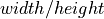
- <interposer_cut x="expr" y="expr"/>" title="Link to this definition">
- Optional Attributes:
x – Specifies the x-coordinate of a vertical interposer cut. Value is an expression (see Grid Location Expressions); variables
WandHare device width and height.y – Specifies the y-coordinate of a horizontal interposer cut. Value is an expression (see Grid Location Expressions); variables
WandHare device width and height.
Note
Exactly one of the
xoryattributes must be specified.Defines an interposer cut for modelling 2.5D interposer-based architectures. An interposer cut will cut all connections at the given location along the specified axis, leaving the two sides completely unconnected. To reconnect the two sides, this tag can have multiple
<interdie_wire>tags as children to specify the connection between the two sides. This tag may appear inside<auto_layout>or<fixed_layout>as a grid location tag.
- <interdie_wire sg_name="string" sg_link="string" offset_start="int" offset_end="int" offset_increment="int" num="expr"/>" title="Link to this definition">
- Required Attributes:
sg_name – Name of the scatter-gather pattern to be used for the interdie connection.
sg_link – Name of the scatter-gather link to be used for the interdie connection.
offset_start – Starting point of scatter-gather instantiations. Must be smaller than ‘offset_end’.
offset_end – Ending point of scatter-gather instantiations. Must be larger than ‘offset_start’.
offset_increment – Increment/distance between scatter-gather instantiations. Must be a positive number.
num – Number of scatter-gather instantiations per switchblock location. May be an integer or a formula; the variable
Wdenotes the routing channel width when the expression is evaluated.
Defines the interdie wiring between the two sides of the cut. Connectivity is defined using scatter-gather patterns. Starting at ‘offset_start’ from location of the cut and moving by ‘offset_increment’ until we reach the location of ‘offset_end’ away from the cut, ‘num’ scatter-gather patterns defined by ‘sg_name’ and ‘sg_link’ will be instantiated. Note that these offset points always define the starting point of the scatter-gather pattern’s sg_link. offset_start, offset_end and offset_increment are integer values.
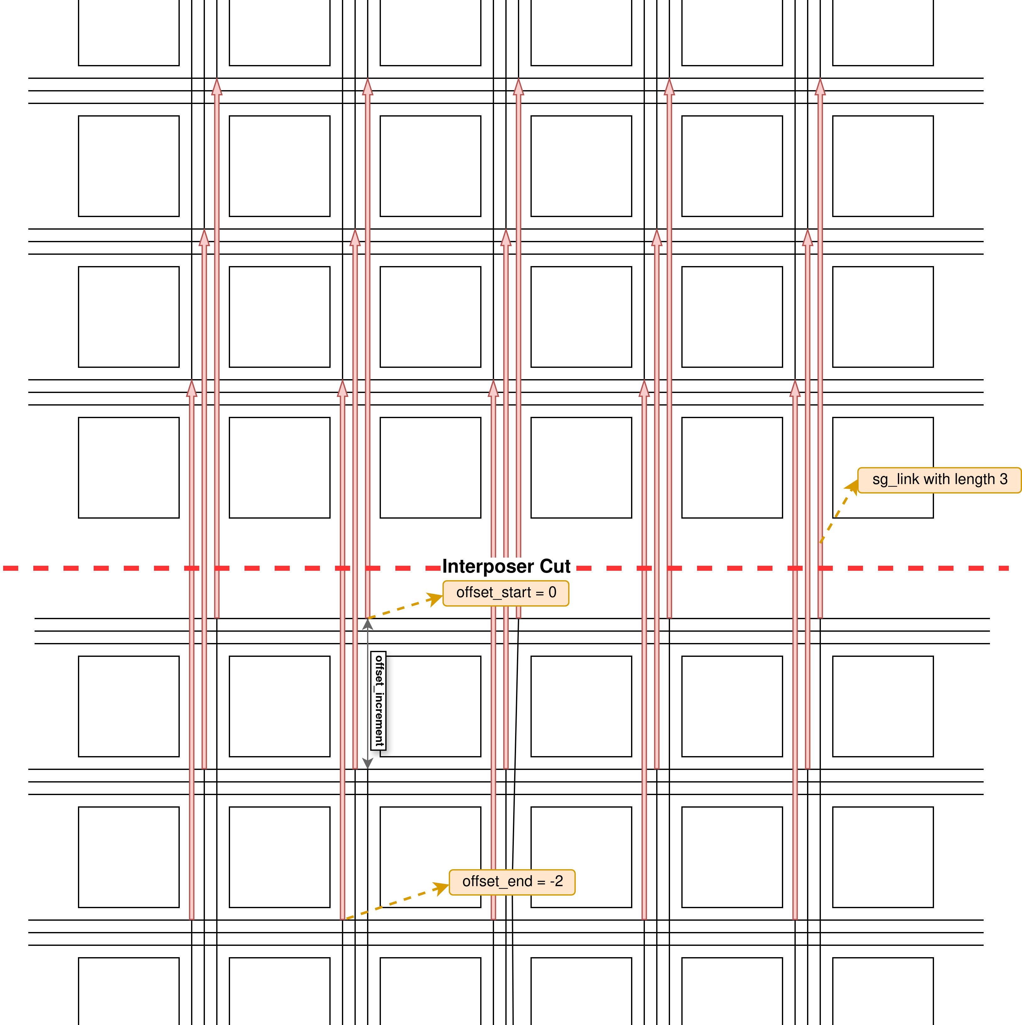
Fig. 26 An example of how specifying interposers in VTR works. Connections between the two sides of a cut are first severed after which the two sides are reconnected using scatter_gather patterns. In this example the length of the sg_link wire used is 3. Note that there are ‘num’ of each pattern at each switchblock location.
FPGA Device Information
The tags within the <device> tag are:
- <sizing R_minW_nmos="float" R_minW_pmos="float"/>" title="Link to this definition">
- Required Attributes:
R_minW_nmos – The resistance of minimum-width nmos transistor. This data is used only by the area model built into VPR.
R_minW_pmos – The resistance of minimum-width pmos transistor. This data is used only by the area model built into VPR.
- Required:
Yes
Specifies parameters used by the area model built into VPR.
- <connection_block input_switch_name="string"/>" title="Link to this definition">
Fig. 27 Input Pin Diagram.
- Required Attributes:
switch_name – Specifies the name of the
<switch>in the<switchlist>used to connect routing tracks to block input pins (i.e. the input connection block switch).
- Required:
Yes
- <area grid_logic_tile_area="float"/>" title="Link to this definition">
- Required:
Yes
Specifies the default area used by each 1x1 grid logic tile (in MWTAs), excluding routing.
Used for an area estimate of the amount of area taken by all the functional blocks.
Note
This value can be overridden for specific
<pb_type>s with theareaattribute.
- <switch_block type="{wilton | subset | universal | custom}" fs="int"/>" title="Link to this definition">
- Required Attributes:
type – The type of switch block to use.
fs – The value of

- Required:
Yes
This parameter controls the pattern of switches used to connect the (inter-cluster) routing segments. Three fairly simple patterns can be specified with a single keyword each, or more complex custom patterns can be specified.
Non-Custom Switch Blocks:
When using bidirectional segments, all the switch blocks have
= 3 [BFRV92].
That is, whenever horizontal and vertical channels intersect, each wire segment can connect to three other wire segments.
The exact topology of which wire segment connects to which can be one of three choices.
The subset switch box is the planar or domain-based switch box used in the Xilinx 4000 FPGAs – a wire segment in track 0 can only connect to other wire segments in track 0 and so on.
The wilton switch box is described in [Wil97], while the universal switch box is described in [CWW96].
To see the topology of a switch box, simply hit the “Toggle RR” button when a completed routing is on screen in VPR.
In general the wilton switch box is the best of these three topologies and leads to the most routable FPGAs.When using unidirectional segments, one can specify an
that is any multiple of 3.
We use a modified wilton switch block pattern regardless of the specified switch_block_type.
For all segments that start/end at that switch block, we follow the wilton switch block pattern.
For segments that pass through the switch block that can also turn there, we cannot use the wilton pattern because a unidirectional segment cannot be driven at an intermediate point, so we assign connections to starting segments following a round robin scheme (to balance mux size).Note
The round robin scheme is not tileable.
Custom Switch Blocks:
Specifying
customallows custom switch blocks to be described under the<switchblocklist>XML node, the format for which is described in Custom Switch Blocks. If the switch block is specified ascustom, thefsfield does not have to be specified, and will be ignored if present.
- <chan_width_distr>content</chan_width_distr>
Content inside this tag is only used when VPR is in global routing mode. The contents of this tag are described in Global Routing Information.
- <default_fc in_type="{frac|abs}" in_val="{int|float}" out_type="{frac|abs}" out_val="{int|float}"/>" title="Link to this definition">
This defines the default Fc specification, if it is not specified within a
<fc>tag inside a top-level complex block. The attributes have the same meaning as the <fc> tag attributes.
- <opin_chanz_connectivity type="{per_side | per_block}"/>" title="Link to this definition">
- Required Attributes:
type –
Specifies how Output Pins (OPINs) connect to CHANZ (inter-layer) nodes via switch blocks in 3D architectures.
per_side: Each side’s OPINs connect to the two Switch Blocks at the corners of that side.per_block: All OPINs from all four sides connect exclusively to the Top-Right Switch Block.
- Required:
Required for architectures utilizing OPIN-to-CHANZ connectivity.
Defines the connectivity pattern between the block output pins and the Z-direction routing channels.
Note
This tag must be defined in architectures where there is OPIN-CHANZ connectivity. If OPINs are not connected to CHANZ, or if the architecture is 2D, this tag does not impact the RR-graph generation.
Switches
The tags within the <switchlist> tag specifies the switches used to connect wires and pins together.
- <switch type="{mux|tristate|pass_gate|short|buffer}" name="string" R="float" Cin="float" Cout="float" Cinternal="float" Tdel="float" buf_size="{auto|float}" mux_trans_size="float", power_buf_size="int"/>" title="Link to this definition">
Describes a switch in the routing architecture.
Example:
<switch type="mux" name="my_awesome_mux" R="551" Cin=".77e-15" Cout="4e-15" Cinternal="5e-15" Tdel="58e-12" mux_trans_size="2.630740" buf_size="27.645901"/>
- Required Attributes:
type –
The type of switch:
mux: An isolating, configurable multiplexertristate: An isolating, configurable tristate-able bufferpass_gate: A non-isolating, configurable pass gateshort: A non-isolating, non-configurable electrical short (e.g. between two segments).buffer: An isolating, non-configurable non-tristate-able buffer (e.g. in-line along a segment).
Isolation
Isolating switches include a buffer which partition their input and output into separate DC-connected sub-circuits. This helps reduce RC wire delays.
Non-isolating switch do not isolate their input and output, which can increase RC wire delays.
Configurablity
Configurable switches can be turned on/off at configuration time.
Non-configurable switches can not be controlled at configuration time. These are typically used to model non-optional connections such as electrical shorts and in-line buffers.
name – A unique name identifying the switch
R – Resistance of the switch.
Cin –
Input capacitance of the switch.
Note
For
shorttype switches,Cinmay be omitted and defaults to0.Cout –
Output capacitance of the switch.
Note
For
shorttype switches,Coutmay be omitted and defaults to0.
- Optional Attributes:
Cinternal –
Since multiplexers and tristate buffers are modeled as a parallel stream of pass transistors feeding into a buffer, we would expect an additional “internal capacitance” to arise when the pass transistor is enabled and the signal must propagate to the buffer. See diagram of one stream below:
Pass Transistor
          |
        -----
        -----      Buffer
       |     |       |\
 ------       -------| \--------
   |             |   | /    |
 =====         ===== |/   =====
 =====         =====      =====
   |             |          |
 Input C    Internal C    Output C
Note
Only specify a value for multiplexers and/or tristate switches.
Tdel –
Intrinsic delay through the switch. If this switch was driven by a zero resistance source, and drove a zero capacitance load, its delay would be:
 .
.The ‘switch’ includes both the mux and buffer
muxtype switches.Note
Required if no
<Tdel>tags are specifiedNote
A
<switch>’s resistance (R) and output capacitance (Cout) have no effect on delay when used for the input connection block, since VPR does not model the resistance/capacitance of block internal wires.buf_size –
Specifies the buffer size in minimum-width transistor area (:term`MWTA`) units.
If set to
auto, sized automatically from the R value. This allows you to use timing models without R’s and C’s and still be able to measure area.Note
Required for all isolating switch types.
Default:
automux_trans_size –
Specifies the size (in minimum width transistors) of each transistor in the two-level mux used by
muxtype switches.Note
Valid only for
muxtype switches.power_buf_size – Used for power estimation. The size is the drive strength of the buffer, relative to a minimum-sized inverter.
- <Tdel num_inputs="int" delay="float"/>" title="Link to this definition">
Instead of specifying a single Tdel value, a list of Tdel values may be specified for different values of switch fan-in. Delay is linearly extrapolated/interpolated for any unspecified fanins based on the two closest fanins.
- Required Attributes:
num_inputs – The number of switch inputs (fan-in)
delay – The intrinsic switch delay when the switch topology has the specified number of switch inputs
Example:
<switch type="mux" name="my_mux" R="522" Cin="3.1e-15" Cout="3e-15" Cinternal="5e-15" mux_trans_size="1.7" buf_size="23">
    <Tdel num_inputs="12" delay="8.00e-11"/>
    <Tdel num_inputs="15" delay="8.4e-11"/>
    <Tdel num_inputs="20" delay="9.4e-11"/>
</switch>
Global Routing Information
If global routing is to be performed, channels in different directions and in different parts of the FPGA can be set to different relative widths.
This is specified in the content within the <chan_width_distr> tag.
Note
If detailed routing is to be performed, only uniform distributions may be used
- <x distr="{gaussian|uniform|pulse|delta}" peak="float" width=" float" xpeak=" float" dc=" float"/>" title="Link to this definition">
- Required Attributes:
distr – The channel width distribution function
peak – The peak value of the distribution
- Optional Attributes:
width – The width of the distribution. Required for
pulseandgaussian.xpeak – Peak location horizontally. Required for
pulse,gaussiananddelta.dc – The DC level of the distribution. Required for
pulse,gaussiananddelta.
Sets the distribution of tracks for the x-directed channels – the channels that run horizontally.
Most values are from 0 to 1.
If uniform is specified, you simply specify one argument, peak. This value (by convention between 0 and 1) sets the width of the x-directed core channels relative to the y-directed channels and the channels between the pads and core. Fig. 28 should clarify the specification of uniform (dashed line) and pulse (solid line) channel widths. The gaussian keyword takes the same four parameters as the pulse keyword, and they are all interpreted in exactly the same manner except that in the gaussian case width is the standard deviation of the function.
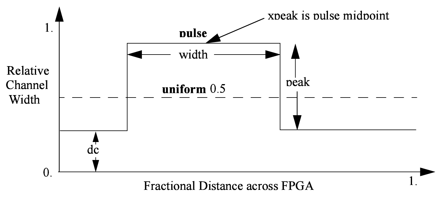
Fig. 28 Channel Distribution
The delta function is used to specify a channel width distribution in which all the channels have the same width except one. The syntax is chan_width_x delta peak xpeak dc. Peak is the extra width of the single wide channel. Xpeak is between 0 and 1 and specifies the location within the FPGA of the extra-wide channel – it is the fractional distance across the FPGA at which this extra-wide channel lies. Finally, dc specifies the width of all the other channels. For example, the statement chan_width_x delta 3 0.5 1 specifies that the horizontal channel in the middle of the FPGA is four times as wide as the other channels.
Examples:
<x distr="uniform" peak="1"/>
<x distr="gaussian" width="0.5" peak="0.8" xpeak="0.6" dc="0.2"/>
Physical Tiles
The content within the <tiles> describes the physical tiles available in the FPGA.
Each tile type is specified with the <tile> tag within the <tiles> tag.
Tile
- <tile name="string" width="int" height="int" area="float"/>" title="Link to this definition">
A tile refers to a placeable element within an FPGA architecture and describes its physical compositions on the grid. The following attributes are applicable to each tile. The only required one is the name of the tile.
Attributes:
- Required Attributes:
name –
The name of this tile.
The name must be unique with respect to any other sibling
<tile>tag.
- Optional Attributes:
width –
The width of the block type in grid tiles
Default:
1height –
The height of the block type in grid tiles
Default:
1area –
The logic area (in MWTA) of the block type
Default: from the
<area>tag
The following tags are common to all <tile> tags:
- <sub_tile name="string" capacity="{int}">" title="Link to this definition">
See also
For a tutorial on describing the usage of sub tiles for
heterogeneous tiles(tiles which support multiple instances of the same or different Complex Blocks) definition see Heterogeneous tiles tutorial.Describes one or many sub tiles corresponding to the physical tile. Each sub tile is identifies a set of one or more stack location on a specific x, y grid location.
Attributes:
- Required Attributes:
name –
The name of this sub tile.
The name must be unique with respect to any other sibling
<sub_tile>tag.
- Optional Attributes:
capacity –
The number of instances of this block type at each grid location.
Default:
1For example:
<sub_tile name="IO" capacity="2"/>
    ...
</sub_tile>
specifies there are two instances of the block type
IOat each of its grid locations.
Note
It is mandatory to have at least one sub tile definition for each physical tile.
- <input name="string" num_pins="int" equivalent="{none|full}" is_non_clock_global="{true|false}"/>" title="Link to this definition">
Defines an input port. Multiple input ports are described using multiple
<input>tags.- Required Attributes:
name – Name of the input port.
num_pins – Number of pins the input port has.
- Optional Attributes:
equivalent –
Describes if the pins of the port are logically equivalent. Input logical equivalence means that the pin order can be swapped without changing functionality. For example, an AND gate has logically equivalent inputs because you can swap the order of the inputs and it’s still correct; an adder, on the otherhand, is not logically equivalent because if you swap the MSB with the LSB, the results are completely wrong. LUTs are also considered logically equivalent since the logic function (LUT mask) can be rotated to account for pin swapping.
none: No input pins are logically equivalent.Input pins can not be swapped by the router. (Generates a unique SINK rr-node for each block input port pin.)
full: All input pins are considered logically equivalent (e.g. due to logical equivalence or a full-crossbar within the cluster).All input pins can be swapped without limitation by the router. (Generates a single SINK rr-node shared by all input port pins.)
default:
noneis_non_clock_global –
Note
Applies only to top-level pb_type.
Describes if this input pin is a global signal that is not a clock. Very useful for signals such as FPGA-wide asynchronous resets. These signals have their own dedicated routing channels and so should not use the general interconnect fabric on the FPGA.
- <output name="string" num_pins="int" equivalent="{none|full|instance}"/>" title="Link to this definition">
Defines an output port. Multiple output ports are described using multiple
<output>tags- Required Attributes:
name – Name of the output port.
num_pins – Number of pins the output port has.
- Optional Attributes:
equivalent –
Describes if the pins of the output port are logically equivalent:
none: No output pins are logically equivalent.Output pins can not be swapped by the router. (Generates a unique SRC rr-node for each block output port pin.)
full: All output pins are considered logically equivalent.All output pins can be swapped without limitation by the router. For example, this option would be appropriate to model an output port which has a full crossbar between it and the logic within the block that drives it. (Generates a single SRC rr-node shared by all output port pins.)
instance: Models that sub-instances within a block (e.g. LUTs/BLEs) can be swapped to achieve a limited form of output pin logical equivalence.Like
full, this generates a single SRC rr-node shared by all output port pins. However, each net originating from this source can use only one output pin from the equivalence group. This can be useful in modeling more complex forms of equivalence in which you can swap which BLE implements which function to gain access to different inputs.Warning
When using
instanceequivalence you must be careful to ensure output swapping would not make the cluster internal routing (previously computed by the clusterer) illegal; the tool does not update the cluster internal routing due to output pin swapping.
Default:
none
- <clock name="string" num_pins="int" equivalent="{none|full}"/>" title="Link to this definition">
Describes a clock port. Multiple clock ports are described using multiple
<clock>tags. See above descriptions on inputs
- <equivalent_sites>
See also
For a step-by-step walkthrough on describing equivalent sites see Equivalent Sites tutorial.
Describes the Complex Blocks that can be placed within a tile. Each physical tile can comprehend a number from 1 to N of possible Complex Blocks, or
sites. Asitecorresponds to a top-level Complex Block that must be placeable in at least 1 physical tile locations.- Required Attributes:
pb_type – Name of the corresponding pb_type.
- Optional Attributes:
pin_mapping –
Specifies whether the pin mapping between physical tile and logical pb_type:
direct: the pin mapping does not need to be specified as the tile pin definition is equal to the corresponding pb_type one;custom: the pin mapping is user-defined.
Default:
directExample: Equivalent Sites
<equivalent_sites>
    <site pb_type="MLAB_SITE" pin_mapping="direct"/>
</equivalent_sites>
- <direct from="string" to="string">" title="Link to this definition">
Describes the mapping of a physical tile’s port on the logical block’s (pb_type) port.
directis an option sub-tag ofsite.Note
This tag is needed only if the pin_mapping of the
siteis defined ascustom- Attributes:
fromis relative to the physical tile pinstois relative to the logical block pins
<direct from="MLAB_TILE.CX" to="MLAB_SITE.BX"/>
- <fc in_type="{frac|abs}" in_val="{int|float}" out_type="{frac|abs}" out_val="{int|float}">" title="Link to this definition">
- Required Attributes:
in_type –
Indicates how the
 values for input pins should be interpreted.
frac: The fraction of tracks of each wire/segment type.abs: The absolute number of tracks of each wire/segment type.in_val – Fraction or absolute number of tracks to which each input pin is connected.
out_type –
Indicates how the
values for output pins should be interpreted.frac: The fraction of tracks of each wire/segment type.abs: The absolute number of tracks of each wire/segment type.out_val – Fraction or absolute number of wires/segments to which each output pin connects.
Sets the number of tracks/wires to which each logic block pin connects in each channel bordering the pin.
The
value [BFRV92] is interpreted as applying to each wire/segment type individually (see example).When generating the FPGA routing architecture VPR will try to make ‘good’ choices about how pins and wires interconnect; for more details on the criteria and methods used see [BR00].
Note
If
<fc>is not specified for a complex block, the architecture’s<default_fc>is used.Note
For unidirection routing architectures absolute
values must be a multiple of 2.Example:
Consider a routing architecture with 200 length 4 (L4) wires and 50 length 16 (L16) wires per channel, and the following Fc specification:
<fc in_type="frac" in_val="0.1" out_type="abs" out_val="25">
The above specifies that each:
input pin connects to 20 L4 tracks (10% of the 200 L4s) and 5 L16 tracks (10% of the 50 L16s), and
output pin connects to 25 L4 tracks and 25 L16 tracks.
Overriding Values:
- <fc_override fc_type="{frac|abs}" fc_val="{int|float}", port_name="{string}" segment_name="{string}">" title="Link to this definition">
Allows
values to be overridden on a port or wire/segment type basis.- Required Attributes:
fc_type –
Indicates how the override
value should be interpreted.frac: The fraction of tracks of each wire/segment type.abs: The absolute number of tracks of each wire/segment type.fc_val – Fraction or absolute number of tracks in a channel.
- Optional Attributes:
port_name – The name of the port to which this override applies. If left unspecified this override applies to all ports.
segment_name – The name of the segment (defined under
<segmentlist>) to which this override applies. If left unspecified this override applies to all segments.
Note
At least one of
port_nameorsegment_namemust be specified.Port Override Example: Carry Chains
If you have complex block pins that do not connect to general interconnect (eg. carry chains), you would use the
<fc_override>tag, within the<fc>tag, to specify them:<fc_override fc_type="frac" fc_val="0" port_name="cin"/> <fc_override fc_type="frac" fc_val="0" port_name="cout"/>
Where the attribute
port_nameis the name of the pin (cinandcoutin this example).Segment Override Example:
It is also possible to specify per
<segment>(i.e. routing wire) overrides:<fc_override fc_type="frac" fc_val="0.1" segment_name="L4"/>
Where the above would cause all pins (both inputs and outputs) to use a fractional
of 0.1when connecting to segments of typeL4.Combined Port and Segment Override Example:
The
port_nameandsegment_nameattributes can be used together. For example:<fc_override fc_type="frac" fc_val="0.1" port_name="my_input" segment_name="L4"/> <fc_override fc_type="frac" fc_val="0.2" port_name="my_output" segment_name="L4"/>
specifies that port
my_inputuse a fractional of 0.1when connecting to segments of typeL4, while the portmy_outputuses a fractional of 0.2when connecting to segments of typeL4. All other port/segment combinations would use the default values.
- <pinlocations pattern="{spread|perimeter|spread_inputs_perimeter_outputs|custom}">" title="Link to this definition">
- Required Attributes:
pattern –
spreaddenotes that the pins are to be spread evenly on all sides of the complex block.Note
Includes internal sides of blocks with width > 1 and/or height > 1.
perimeterdenotes that the pins are to be spread evenly on perimeter sides of the complex block.Note
Excludes the internal sides of blocks with width > 1 and/or height > 1.
spread_inputs_perimeter_outputsdenotes that input pins are to be spread on all sides of the complex block, but output pins are to be spread only on perimeter sides of the block.Note
This is useful for ensuring outputs do not connect to wires which fly-over a width > 1 and height > 1 block (e.g. if using
shortorbufferconnections instead of a fully configurable switch block within the block).customallows the architect to specify specifically where the pins are to be placed using<loc>tags.
Describes the locations where the input, output, and clock pins are distributed in a complex logic block.
- <loc side="{left|right|bottom|top}" xoffset="int" yoffset="int">name_of_complex_logic_block.port_name[int:int] ... </loc>name_of_complex_logic_block.port_name[int:int]..." title="Link to this definition">
Note
...represents repeat as needed. Do not put...in the architecture file.- Required Attributes:
side – Specifies which of the four sides of a grid location the pins in the contents are located.
- Optional Attributes:
xoffset –
Specifies the horizontal offset (in grid units) from block origin (bottom left corner). The offset value must be less than the width of the block.
Default:
0yoffset –
Specifies the vertical offset (in grid units) from block origin (bottom left corner). The offset value must be less than the height of the block.
Default:
0
If the subtile capacity is greater than 1, you can specify the capacity range when defining the pin locations. For example:
<sub_tile name="io_bottom" capacity="6">
    <equivalent_sites>
        <site pb_type="io"/>
    </equivalent_sites>
    <input name="outpad" num_pins="1"/>
    <output name="inpad" num_pins="1"/>
    <fc in_type="frac" in_val="0.15" out_type="frac" out_val="0.10"/>
    <pinlocations pattern="custom">
        <loc side="top">io_bottom[0:1].outpad io_bottom[0:3].inpad io_bottom[2:5].outpad io_bottom[4:5].inpad</loc>
    </pinlocations>
</sub_tile>
If no capacity range is specified, it is assumed that the location applies to all capacity instances.
Physical equivalence for a pin is specified by listing a pin more than once for different locations. For example, a LUT whose output can exit from the top and bottom of a block will have its output pin specified twice: once for the top and once for the bottom.
A
<loc>tag may have empty content (no pin strings), which indicates that no pins are located on that side at the specified offset. This is useful when explicitly marking a side as having no pins, for example in heterogeneous tiles where some sides are intentionally left unconnected.Note
If the
<pinlocations>tag is missing, aspreadpattern is assumed.
- <switchblock_locations pattern="{external_full_internal_straight|all|external|internal|none|custom}" internal_switch="string">" title="Link to this definition">
Describes where global routing switchblocks are created in relation to the complex block.
Note
If the
<switchblock_locations>tag is left unspecified the default pattern is assumed.- Optional Attributes:
pattern –
external_full_internal_straight: creates full switchblocks outside and straight switchblocks inside the complex blockall: creates switchblocks wherever routing channels crossexternal: creates switchblocks wherever routing channels cross outside the complex blockinternal: creates switchblocks wherever routing channels cross inside the complex blocknone: denotes that no switchblocks are created for the complex blockcustom: allows the architect to specify custom switchblock locations and types using<sb_loc>tags
Default:
external_full_internal_straight

Fig. 29 Switchblock Location Patterns for a width = 2, height = 3 complex block
- Optional Attributes:
internal_switch –
The name of a switch (from
<switchlist>) which should be used for internal switch blocks.Default: The default switch for the wire
<segment>Note
This is typically used to specify that internal wire segments are electrically shorted together using a
shorttype<switch>.
Example: Electrically Shorted Internal Straight Connections
In some architectures there are no switch blocks located ‘within’ a block, and the wires crossing over the block are instead electrcially shorted to their ‘straight-through’ connections.
To model this we first define a special
shorttype switch to electrically short such segments together:<switchlist> <switch type="short" name="electrical_short" R="0" Cin="0" Tdel="0"/> </switchlist>
Next, we use the pre-defined
external_full_internal_straightpattern, and that such connections should use ourelectrical_shortswitch.<switchblock_locations pattern="external_full_internal_straight" internal_switch="electrical_short"/>
- <sb_loc type="{full|straight|turns|horizontal|vertical|horizontal_short|vertical_short|straight_short|none}" xoffset="int" yoffset="int", switch_override="string">" title="Link to this definition">
Specifies the type of switchblock to create at a particular location relative to a complex block for the
customswitchblock location pattern.- Required Attributes:
type –
Specifies the type of switchblock to be created at this location:
full: denotes that a full switchblock will be created (i.e. bothstraightandturns)straight: denotes that a switchblock with only straight connections will be created (i.e. noturns)turns: denotes that a switchblock with only turning connections will be created (i.e. nostraight)horizontal: denotes that a switchblock with only horizontal straight connections will be created (i.e. CHANX to CHANX only)vertical: denotes that a switchblock with only vertical straight connections will be created (i.e. CHANY to CHANY only)horizontal_short: likehorizontal, but connects only wires with the same track number (ptc) using the delayless switchvertical_short: likevertical, but connects only wires with the same track number (ptc) using the delayless switchstraight_short: likestraight, but connects only wires with the same track number (ptc) using the delayless switchnone: denotes that no switchblock will be created
Default:
fullNote
The
*_shorttypes are only supported for uni-directional routing graphs. They are typically used to model electrical shorts at locations such as TSV holes in 3D architectures, where wires cross the TSV hole straight-through.
Fig. 30 Switchblock Types
- Optional Attributes:
xoffset –
Specifies the horizontal offset (in grid units) from block origin (bottom left corner). The offset value must be less than the width of the block.
Default:
0yoffset –
Specifies the vertical offset (in grid units) from block origin (bottom left corner). The offset value must be less than the height of the block.
Default:
0switch_override –
The name of a switch (from
<switchlist>) which should be used to construct the switch block at this location.Default: The default switch for the wire
<segment>
Note
The switchblock associated with a grid tile is located to the top-right of the grid tile
Example: Custom Description of Electrically Shorted Internal Straight Connections
If we assume a width=2, height=3 block (e.g. Fig. 29), we can use a custom pattern to specify an architecture equivalent to the ‘Electrically Shorted Internal Straight Connections’ example:
<switchblock_locations pattern="custom">
    <!-- Internal: using straight electrical shorts -->
    <sb_loc type="straight" xoffset="0" yoffset="0" switch_override="electrical_short">
    <sb_loc type="straight" xoffset="0" yoffset="1" switch_override="electrical_short">

    <!-- External: using default switches -->
    <sb_loc type="full" xoffset="0" yoffset="2"> <!-- Top edge -->
    <sb_loc type="full" xoffset="1" yoffset="0"> <!-- Right edge -->
    <sb_loc type="full" xoffset="1" yoffset="1"> <!-- Right edge -->
    <sb_loc type="full" xoffset="1" yoffset="2"> <!-- Top Right -->
<switchblock_locations/>
Complex Blocks
See also
For a step-by-step walkthrough on building a complex block see Architecture Modeling.
The content within the <complexblocklist> describes the complex blocks found within the FPGA.
Each type of complex block is specified with a top-level <pb_type> tag within the <complexblocklist> tag.
PB Type
- <pb_type name="string" num_pb="int" blif_model="string"/>" title="Link to this definition">
Specifies a top-level complex block, or a complex block’s internal components (sub-blocks). Which attributes are applicable depends on where the
<pb_type>tag falls within the hierarchy:Top Level: A child of the
<complexblocklist>Intermediate: A child of another
<pb_type>Primitive/Leaf: Contains no
<pb_type>children
For example:
<complexblocklist>
    <pb_type name="CLB"/> <!-- Top level -->
        ...
        <pb_type name="ble"/> <!-- Intermediate -->
            ...
            <pb_type name="lut"/> <!-- Primitive -->
                ...
            </pb_type>
            <pb_type name="ff"/> <!-- Primitive -->
                ...
            </pb_type>
            ...
        </pb_type>
        ...
    </pb_type>
    ...
</complexblocklist>
General:
- Required Attributes:
name –
The name of this pb_type.
The name must be unique with respect to any parent, sibling, or child
<pb_type>.
Top-level, Intermediate or Primitive:
- Optional Attributes:
num_pb –
The number of instances of this pb_type at the current hierarchy level.
Default:
1For example:
<pb_type name="CLB">
    ...
    <pb_type name="ble" num_pb="10"/>
       ...
    </pb_type>
    ...
</pb_type>
would specify that the pb_type
CLBcontains 10 instances of theblepb_type.
Primitive Only:
- Required Attributes:
blif_model –
Specifies the netlist primitive which can be implemented by this pb_type.
Accepted values:
.input: A BLIF netlist input.output: A BLIF netlist output.names: A BLIF .names (LUT) primitive.latch: A BLIF .latch (DFF) primitive.subckt <custom_type>: A user defined black-box primitive.
For example:
<pb_type name="my_adder" blif_model=".subckt adder"/>
   ...
</pb_type>
would specify that the pb_type
my_addercan implement a black-box BLIF primitive namedadder.Note
The input/output/clock ports for primitive pb_types must match the ports specified in the
<models>section.
- Optional Attributes:
class –
Specifies that this primitive is of a specialized type which should be treated specially.
See also
Classes for more details.
The following tags are common to all <pb_type> tags:
- <input name="string" num_pins="int" equivalent="{none|full}" is_non_clock_global="{true|false}"/>" title="Link to this definition">
Defines an input port. Multiple input ports are described using multiple
<input>tags.- Required Attributes:
name – Name of the input port.
num_pins – Number of pins the input port has.
- Optional Attributes:
equivalent –
Note
Applies only to top-level pb_type.
Describes if the pins of the port are logically equivalent. Input logical equivalence means that the pin order can be swapped without changing functionality. For example, an AND gate has logically equivalent inputs because you can swap the order of the inputs and it’s still correct; an adder, on the otherhand, is not logically equivalent because if you swap the MSB with the LSB, the results are completely wrong. LUTs are also considered logically equivalent since the logic function (LUT mask) can be rotated to account for pin swapping.
none: No input pins are logically equivalent.Input pins can not be swapped by the router. (Generates a unique SINK rr-node for each block input port pin.)
full: All input pins are considered logically equivalent (e.g. due to logical equivalence or a full-crossbar within the cluster).All input pins can be swapped without limitation by the router. (Generates a single SINK rr-node shared by all input port pins.)
default:
noneis_non_clock_global –
Note
Applies only to top-level pb_type.
Describes if this input pin is a global signal that is not a clock. Very useful for signals such as FPGA-wide asynchronous resets. These signals have their own dedicated routing channels and so should not use the general interconnect fabric on the FPGA.
- <output name="string" num_pins="int" equivalent="{none|full|instance}"/>" title="Link to this definition">
Defines an output port. Multiple output ports are described using multiple
<output>tags- Required Attributes:
name – Name of the output port.
num_pins – Number of pins the output port has.
- Optional Attributes:
equivalent –
Note
Applies only to top-level pb_type.
Describes if the pins of the output port are logically equivalent:
none: No output pins are logically equivalent.Output pins can not be swapped by the router. (Generates a unique SRC rr-node for each block output port pin.)
full: All output pins are considered logically equivalent.All output pins can be swapped without limitation by the router. For example, this option would be appropriate to model an output port which has a full crossbar between it and the logic within the block that drives it. (Generates a single SRC rr-node shared by all output port pins.)
instance: Models that sub-instances within a block (e.g. LUTs/BLEs) can be swapped to achieve a limited form of output pin logical equivalence.Like
full, this generates a single SRC rr-node shared by all output port pins. However, each net originating from this source can use only one output pin from the equivalence group. This can be useful in modeling more complex forms of equivalence in which you can swap which BLE implements which function to gain access to different inputs.Warning
When using
instanceequivalence you must be careful to ensure output swapping would not make the cluster internal routing (previously computed by the clusterer) illegal; the tool does not update the cluster internal routing due to output pin swapping.
Default:
none
- <clock name="string" num_pins="int" equivalent="{none|full}"/>" title="Link to this definition">
Describes a clock port. Multiple clock ports are described using multiple
<clock>tags. See above descriptions on inputs
- <mode name="string" disable_packing="bool">" title="Link to this definition">
- Required Attributes:
name – Name for this mode. Must be unique compared to other modes.
Specifies a mode of operation for the
<pb_type>. Each child mode tag denotes a different mode of operation for the<pb_type>. Each mode tag may contain other<pb_type>and<interconnect>tags.Note
Modes within the same parent
<pb_type>are mutually exclusive.Note
If a
<pb_type>has only one mode of operation the mode tag can be omitted.- Optional Attributes:
disable_packing – Specify if a mode is disabled or not for VPR packer. When a mode is defined to be disabled for packing (
disable_packing="true"), packer will not map any logic to the mode. This optional syntax aims to help debugging of multi-mode<pb_type>so that users can spot bugs in their XML definition quickly. By default, it is set tofalse.
Note
When a mode is specified to be disabled for packing, its child
<pb_type>and the<mode>of child<pb_type>will be considered as disabled for packing automatically. There is no need to specifydisable_packingfor every<mode>in the tree of<pb_type>.Warning
This is a power-user debugging option. See Multi-mode Logic Block Tutorial for a detailed how-to-use.
For example:
<!--A fracturable 6-input LUT-->
<pb_type name="lut">
    ...
    <mode name="lut6">
        <!--Can be used as a single 6-LUT-->
        <pb_type name="lut6" num_pb="1">
            ...
        </pb_type>
        ...
    </mode>
    ...
    <mode name="lut5x2">
        <!--Or as two 5-LUTs-->
        <pb_type name="lut5" num_pb="2">
            ...
        </pb_type>
        ...
    </mode>
</pb_type>
specifies the
lutpb_type can be used as either a single 6-input LUT, or as two 5-input LUTs (but not both).
Interconnect
As mentioned earlier, the mode tag contains <pb_type> tags and an <interconnect> tag.
The following describes the tags that are accepted in the <interconnect> tag.
- <complete name="string" input="string" output="string"/>" title="Link to this definition">
- Required Attributes:
name – Identifier for the interconnect.
input – Pins that are inputs to this interconnect.
output – Pins that are outputs of this interconnect.
Describes a fully connected crossbar. Any pin in the inputs can connect to any pin at the output.
Example:
<complete input="Top.in" output="Child.in"/>
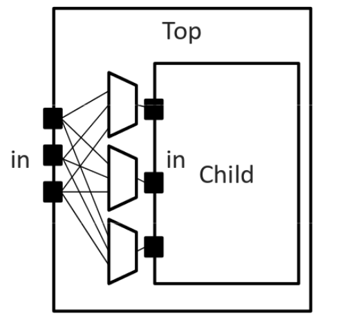
Fig. 31 Complete interconnect example.
- <direct name="string" input="string" output="string"/>" title="Link to this definition">
- Required Attributes:
name – Identifier for the interconnect.
input – Pins that are inputs to this interconnect.
output – Pins that are outputs of this interconnect.
Describes a 1-to-1 mapping between input pins and output pins.
Example:
<direct input="Top.in[2:1]" output="Child[1].in"/>

Fig. 32 Direct interconnect example.
- <mux name="string" input="string" output="string" bus="{true|false}"/>" title="Link to this definition">
- Required Attributes:
name – Identifier for the interconnect.
input – Pins that are inputs to this interconnect. Different data lines are separated by a space.
output – Pins that are outputs of this interconnect.
- Optional Attributes:
bus –
Whether this mux selects between multi-bit (bus) data lines.
When
true, each data line may be a multi-bit bus and the bit width of every mux input must match the bit width of the mux output.When
false(the default), every data line and the output must be a single pin.
Example:
<mux input="Top.A Top.B" output="Child.in"/>

Fig. 33 Mux interconnect example.
Bus-based example:
With
bus="true"each data line may be a multi-bit bus. Every input data line and the output must have the same bit width. In the example below the 27-bit busesone_mult_27x27.aandone_mult_27x27.bare the two data lines selected onto the 27-bit outputmult_27x27.a:<mux name="a2a" input="one_mult_27x27.a one_mult_27x27.b" output="mult_27x27.a" bus="true"/>
A data line may also be a bit-slice of a wider port, or a concatenation of pins using
{...}; in every case the width of each data line must match the output width. Here each data line is a 27-bit slice of the 54-bitmult_27.datainbus:<mux name="datain2a" input="mult_27.datain[26:0] mult_27.datain[53:27]" output="one_mult_27x27.a" bus="true"/>
Note
bus="true"is currently a convenience shorthand: VPR expands it into a set of independent single-bit muxes (one per output bit), rather than modeling a true multi-bit bus. This means each single-bit mux gets its own separate config bit, whereas in a true bus-based mux all of the bit-level muxes would share a single config bit.
A <complete>, <direct>, or <mux> tag may take one or more additional, optional, <pack_pattern> tags that are used to describe molecules.
A pack pattern is a power user feature directing that the CAD tool should group certain netlist atoms (eg. LUTs, FFs, carry chains) together during the CAD flow.
This allows the architect to help the CAD tool recognize structures that have limited flexibility so that netlist atoms that fit those structures be kept together as though they are one unit.
This tag impacts the CAD tool only, there is no architectural impact from defining molecules.
- <pack_pattern name="string" in_port="string" out_port="string"/>" title="Link to this definition">
Warning
This is a power user option. Unless you know why you need it, you probably shouldn’t specify it.
- Required Attributes:
name – The name of the pattern.
in_port – The input pins of the edges for this pattern.
out_port – Which output pins of the edges for this pattern.
This tag gives a hint to the CAD tool that certain architectural structures should stay together during packing. The tag labels interconnect edges with a pack pattern name. All primitives connected by the same pack pattern name become a single pack pattern. Any group of atoms in the user netlist that matches a pack pattern are grouped together by VPR to form a molecule. Molecules are kept together as one unit in VPR. This is useful because it allows the architect to help the CAD tool assign atoms to complex logic blocks that have interconnect with very limited flexibility. Examples of architectural structures where pack patterns are appropriate include: optionally registered inputs/outputs, carry chains, multiply-add blocks, etc.
There is a priority order when VPR groups molecules. Pack patterns with more primitives take priority over pack patterns with less primitives. In the event that the number of primitives is the same, the pack pattern with less inputs takes priority over pack patterns with more inputs.
Special Case:
To specify carry chains, we use a special case of a pack pattern. If a pack pattern has exactly one connection to a logic block input pin and exactly one connection to a logic block output pin, then that pack pattern takes on special properties. The prepacker will assume that this pack pattern represents a structure that spans multiple logic blocks using the logic block input/output pins as connection points. For example, lets assume that a logic block has two, 1-bit adders with a carry chain that links adjacent logic blocks. The architect would specify those two adders as a pack pattern with links to the logic block cin and cout pins. Lets assume the netlist has a group of 1-bit adder atoms chained together to form a 5-bit adder. VPR will break that 5-bit adder into 3 molecules: two 2-bit adders and one 1-bit adder connected in order by a the carry links.
Example:
Consider a classic basic logic element (BLE) that consists of a LUT with an optionally registered flip-flop. If a LUT is followed by a flip-flop in the netlist, the architect would want the flip-flop to be packed with the LUT in the same BLE in VPR. To give VPR a hint that these blocks should be connected together, the architect would label the interconnect connecting the LUT and flip-flop pair as a pack_pattern:
<pack_pattern name="ble" in_port="lut.out" out_port="ff.D"/>
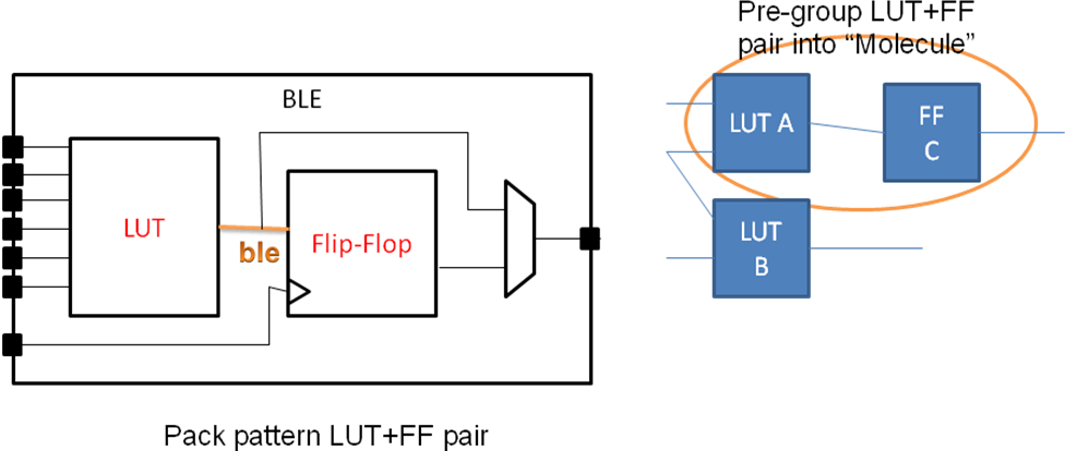
Fig. 34 Pack Pattern Example.
Classes
Using these structures, we believe that one can describe any digital complex logic block.
However, we believe that certain kinds of logic structures are common enough in FPGAs that special shortcuts should be available to make their specification easier.
These logic structures are: flip-flops, LUTs, and memories.
These structures are described using a class=string attribute in the <pb_type> primitive.
The classes we offer are:
- class="lut"
Describes a K-input lookup table.
The unique characteristic of a lookup table is that all inputs to the lookup table are logically equivalent. When this class is used, the input port must have a
port_class="lut_in"attribute and the output port must have aport_class="lut_out"attribute.
- class="flipflop"
Describes a flipflop.
Input port must have a
port_class="D"attribute added. Output port must have aport_class="Q"attribute added. Clock port must have aport_class="clock"attribute added.
- class="memory"
Describes a memory.
Memories are unique in that a single memory physical primitive can hold multiple, smaller, logical memories as long as:
The address, clock, and control inputs are identical and
There exists sufficient physical data pins to satisfy the netlist memories when the different netlist memories are merged together into one physical memory.
Different types of memories require different attributes.
Single Port Memories Require:
An input port with
port_class="address"attributeAn input port with
port_class="data_in"attributeAn input port with
port_class="write_en"attributeAn input port with
port_class="read_en"attribute (optional)An output port with
port_class="data_out"attributeA clock port with
port_class="clock"attribute
Dual Port Memories Require:
An input port with
port_class="address1"attributeAn input port with
port_class="data_in1"attributeAn input port with
port_class="write_en1"attributeAn input port with
port_class="read_en1"attribute (optional)An input port with
port_class="address2"attributeAn input port with
port_class="data_in2"attributeAn input port with
port_class="write_en2"attributeAn input port with
port_class="read_en2"attribute (optional)An output port with
port_class="data_out1"attributeAn output port with
port_class="data_out2"attributeA clock port with
port_class="clock"attribute
Note
Memory port class values support an optional numeric suffix to identify the port’s index (e.g.
address,address1,address2). The un-suffixed form (e.g.address) is equivalent to index 1 (i.e.address1). This generalizes to N-port memories: useaddressN,data_inN,write_enN,read_enN, anddata_outNfor each port index N ≥ 1.
Timing
See also
For examples of primitive timing modeling specifications see the Primitive Block Timing Modeling Tutorial
Timing is specified through tags contained with in pb_type, complete, direct, or mux tags as follows:
- <delay_constant max="float" min="float" in_port="string" out_port="string"/>" title="Link to this definition">
- Optional Attributes:
max – The maximum delay value.
min – The minimum delay value.
- Required Attributes:
in_port – The input port name.
out_port – The output port name.
Specifies a maximum and/or minimum delay from in_port to out_port.
If
in_portandout_portare non-sequential (i.e. combinational), specifies the combinational path delay between them.If
in_portandout_portare sequential (i.e. haveT_setupand/orT_clock_to_Qtags), specifies the combinational delay between the primitive’s input and/or output registers.
Note
At least one of the
maxorminattributes must be specifiedNote
If only one of
maxorminare specified the unspecified value is implicitly set to the same value
- <delay_matrix type="{max | min}" in_port="string" out_port="string"> matrix </delay>matrix" title="Link to this definition">
- Required Attributes:
type – Specifies the delay type.
in_port – The input port name.
out_port – The output port name.
matrix – The delay matrix.
Describe a timing matrix for all edges going from
in_porttoout_port. Number of rows of matrix should equal the number of inputs, number of columns should equal the number of outputs.If
in_portandout_portare non-sequential (i.e. combinational), specifies the combinational path delay between them.If
in_portandout_portare sequential (i.e. haveT_setupand/orT_clock_to_Qtags), specifies the combinational delay between the primitive’s input and/or output registers.
Example: The following defines a delay matrix for a 4-bit input port
in, and 3-bit output portout:<delay_matrix type="max" in_port="in" out_port="out"> 1.2e-10 1.4e-10 3.2e-10 4.6e-10 1.9e-10 2.2e-10 4.5e-10 6.7e-10 3.5e-10 7.1e-10 2.9e-10 8.7e-10 </delay>
Note
To specify both
maxandmindelays two<delay_matrix>should be used.
- <T_setup value="float" port="string" clock="string"/>" title="Link to this definition">
- Required Attributes:
value – The setup time value.
port – The port name the setup constraint applies to.
clock – The port name of the clock the setup constraint is specified relative to.
Specifies a port’s setup constraint.
If
portis an input, specifies the external setup time of the primitive’s input register (i.e. for paths terminating at the input register).If
portis an output, specifies the internal setup time of the primitive’s output register (i.e. for paths terminating at the output register) .
Note
Applies only to primitive
<pb_type>tags
- <T_hold value="float" port="string" clock="string"/>" title="Link to this definition">
- Required Attributes:
value – The hold time value.
port – The port name the setup constraint applies to.
clock – The port name of the clock the setup constraint is specified relative to.
Specifies a port’s hold constraint.
If
portis an input, specifies the external hold time of the primitive’s input register (i.e. for paths terminating at the input register).If
portis an output, specifies the internal hold time of the primitive’s output register (i.e. for paths terminating at the output register) .
Note
Applies only to primitive
<pb_type>tags
- <T_clock_to_Q max="float" min="float" port="string" clock="string"/>" title="Link to this definition">
- Optional Attributes:
max – The maximum clock-to-Q delay value.
min – The minimum clock-to-Q delay value.
- Required Attributes:
port – The port name the delay value applies to.
clock – The port name of the clock the clock-to-Q delay is specified relative to.
Specifies a port’s clock-to-Q delay.
If
portis an input, specifies the internal clock-to-Q delay of the primitive’s input register (i.e. for paths starting at the input register).If
portis an output, specifies the external clock-to-Q delay of the primitive’s output register (i.e. for paths starting at the output register) .
Note
At least one of the
maxorminattributes must be specifiedNote
If only one of
maxorminare specified the unspecified value is implicitly set to the same valueNote
Applies only to primitive
<pb_type>tags
Modeling Sequential Primitive Internal Timing Paths
See also
For examples of primitive timing modeling specifications see the Primitive Block Timing Modeling Tutorial
By default, if only <T_setup> and <T_clock_to_Q> are specified on a primitive pb_type no internal timing paths are modeled.
However, such paths can be modeled by using <delay_constant> and/or <delay_matrix> can be used in conjunction with <T_setup> and <T_clock_to_Q>.
This is useful for modeling the speed-limiting path of an FPGA hard block like a RAM or DSP.
As an example, consider a sequential black-box primitive named seq_foo which has an input port in, output port out, and clock clk:
<pb_type name="seq_foo" blif_model=".subckt seq_foo" num_pb="1">
    <input name="in" num_pins="4"/>
    <output name="out" num_pins="1"/>
    <clock name="clk" num_pins="1"/>

    <!-- external -->
    <T_setup value="80e-12" port="seq_foo.in" clock="clk"/>
    <T_clock_to_Q max="20e-12" port="seq_foo.out" clock="clk"/>

    <!-- internal -->
    <T_clock_to_Q max="10e-12" port="seq_foo.in" clock="clk"/>
    <delay_constant max="0.9e-9" in_port="seq_foo.in" out_port="seq_foo.out"/>
    <T_setup value="90e-12" port="seq_foo.out" clock="clk"/>
</pb_type>
To model an internal critical path delay, we specify the internal clock-to-Q delay of the input register (10ps), the internal combinational delay (0.9ns) and the output register’s setup time (90ps). The sum of these delays corresponds to a 1ns critical path delay.
Note
Primitive timing paths with only one stage of registers can be modeled by specifying <T_setup> and <T_clock_to_Q> on only one of the ports.
Power
See also
Power Estimation, for the complete list of options, their descriptions, and required sub-fields.
- <power method="string">contents</power>contents" title="Link to this definition">
- Optional Attributes:
method –
Indicates the method of power estimation used for the given pb_type.
Must be one of:
specify-sizeauto-sizepin-toggleC-internalabsoluteignoresum-of-children
Default:
auto-size.See also
Power Architecture Modelling for a detailed description of the various power estimation methods.
The
contentsof the tag can consist of the following tags:<dynamic_power><static_power><pin>
- <dynamic_power power_per_instance="float" C_internal="float"/>" title="Link to this definition">
- Optional Attributes:
power_per_instance – Absolute power in Watts.
C_internal – Block capacitance in Farads.
- <static_power power_per_instance="float"/>" title="Link to this definition">
- Optional Attributes:
power_per_instance – Absolute power in Watts.
- <port name="string" energy_per_toggle="float" scaled_by_static_prob="string" scaled_by_static_prob_n="string"/>" title="Link to this definition">
- Required Attributes:
name – Name of the port.
energy_per_toggle – Energy consumed by a toggle on the port specified in
name.
- Optional Attributes:
scaled_by_static_prob – Port name by which to scale
energy_per_togglebased on its logic high probability.scaled_by_static_prob_n – Port name by which to scale
energy_per_togglebased on its logic low probability.
NoC Description
The <noc> tag is an optional tag and its contents allows designers to describe a NoC on an FPGA device.
The <noc> tag is the top level tag for the NoC description and its attributes define the overall properties
of the NoC; refer below for its contents.
- <noc link_bandwidth="float" link_latency="float" router_latency="float" noc_router_tile_name="string">" title="Link to this definition">
- Required Attributes:
link_bandwidth – Specifies the maximum bandwidth in bits-per-second (bps) that a link in the NoC can support
link_latency – Specifies the delay in seconds seen by a flit as it travels from one physical NoC router to another using a NoC link.
router_latency – Specifies the un-loaded delays in seconds as it travels through a physical router.
noc_router_tile_name – Specifies a string which represents the name used to identify a NoC router tile (physical hard block) in the corresponding FPGA architecture. This information is needed to create a model of the NoC.
The <noc> tag contains either a <topology> tag or a <mesh> tag (but not both) which describes the topology of the NoC.
NoC topology
The <topology> tag can be used to specify an arbitrary topology by enumerating each router and its connections.
The <topology> tag consists of multiple <router> tags.
Below is an example of how the <topology> tag is used.
<topology>
    <!--A number of <router> tags go here-->
</topology>
The <router> tag and its contents are described below.
- <router id="int" positionx="float" positiony="float" connections="int int int int ...">" title="Link to this definition">
This tag represents a single physical NoC router on the FPGA device and specifies how it is connected within the NoC.
- Required Attributes:
id – Specifies a user identification (ID) number which is associate to the physical router that this tag is identifying. This ID is used to report errors and warnings to the user.
positionx – Specifies the horizontal position of the physical router block that this tag is identifying. This position does not have to be exact, it can be an approximate value.
positiony – Specifies the vertical position of the physical router block that this tag is identifying. This position does not have to be exact, it can be an approximate value.
connections – Specifies a list of numbers separated by spaces which are the user IDs supplied to other
<router>tags. This describes how the current physical Noc router that this tag is identifying is connected to the other physical NoC routers on the device.
Below is an example of the
<router>tag which identifies a physical router located near (0,0) with ID 0. This router is also connected to two other routers identified by IDs 1 and 2.<router id="0" positionx="0" positiony="0" connections="1 2"/>
NoC mesh topology
As an alternative to the <topology> tag, the <mesh> tag can be used to automatically generate a
uniform 2D mesh NoC topology. The mesh consists of size x size routers per layer, evenly distributed
within the specified rectangular region of the device. Routers are connected to their immediate neighbours
(left, right, above, below, and vertically adjacent layers where applicable).
Router IDs are assigned starting from 0 at the bottom-left corner of the first layer and increasing
in row-major order across layers.
- <mesh startx="float" endx="float" starty="float" endy="float" startlayer="int" endlayer="int" size="int">" title="Link to this definition">
- Required Attributes:
startx – Specifies the horizontal position of the left edge of the rectangular region in which the mesh of NoC routers is placed.
endx – Specifies the horizontal position of the right edge of the rectangular region in which the mesh of NoC routers is placed.
starty – Specifies the vertical position of the bottom edge of the rectangular region in which the mesh of NoC routers is placed.
endy – Specifies the vertical position of the top edge of the rectangular region in which the mesh of NoC routers is placed.
size – Specifies the number of routers along each dimension of the mesh grid. A value of
Nproduces anNxNgrid of routers per layer, for a total ofN * N * (endlayer - startlayer + 1)routers. Must be greater than1.
- Optional Attributes:
startlayer – Specifies the index of the first device layer on which NoC routers are placed. Defaults to
0if not provided.endlayer – Specifies the index of the last device layer on which NoC routers are placed. Defaults to
0if not provided. Must be greater than or equal tostartlayer.
The first and last router in each row or column are positioned on the boundary of the specified region. The remaining routers are evenly spaced within the region.
Below is an example of the
<mesh>tag which creates a 3x3 mesh of NoC routers spanning the device region from (0,0) to (10,10) on a single layer.<mesh startx="0" endx="10" starty="0" endy="10" size="3"/>
NoC Description Example
Below is an example which describes a NoC architecture which has 4 physical routers that are connected to each other to form a
2x2 mesh topology using the <topology> tag.
<!-- Description of a 2x2 mesh NoC-->
<noc link_bandwidth="1.2e9" router_latency="1e-9" link_latency="1e-9" noc_router_tile_name="noc_router_adapter">
    <topology>
            <router id="0" positionx="0" positiony="0" connections="1 2"/>
            <router id="1" positionx="5" positiony="0" connections="0 3"/>
            <router id="2" positionx="0" positiony="5" connections="0 3"/>
            <router id="3" positionx="5" positiony="5" connections="1 2"/>
    </topology>
</noc>
The same 2x2 topology can be described more concisely using the <mesh> tag.
<!-- Description of a 2x2 mesh NoC using the <mesh> tag -->
<noc link_bandwidth="1.2e9" router_latency="1e-9" link_latency="1e-9" noc_router_tile_name="noc_router_adapter">
    <mesh startx="0" endx="5" starty="0" endy="5" size="2"/>
</noc>
Wire Segments
The content within the <segmentlist> tag consists of a group of <segment> tags.
The <segment> tag and its contents are described below.
- <segment axis="{x|y|z}" name="unique_name" length="int" type="{bidir|unidir}" res_type="{GCLK|GENERAL}" freq="float" Rmetal="float" Cmetal="float">content</segment>content" title="Link to this definition">
- Optional Attributes:
axis –
Specifies if the given segment applies to x, y, or z channels only. If this tag is not given, it is assumed that the given segment description applies to both x-directed and y-directed channels (and not to z-directed channels).
Note
It is required that both x and y segment axis details are given or that at least one segment within
segmentlistis specified without theaxistag (i.e. at least one segment applies to both x-directed and y-directed channels). For 3-d architectures, it is required that at least one wire segment with axis=”z” is defined.res_type – Specifies whether the segment belongs to the general or a clock routing network. If this tag is not specified, the resource type for the segment is considered to be GENERAL (i.e. regular routing).
- Required Attributes:
name – A unique alphanumeric name to identify this segment type.
length –
Either the number of logic blocks spanned by each segment, or the keyword
longline. Longline means segments of this type span the entire FPGA array.Note
longlineis only supported forbidirroutingfreq – The supply of routing tracks composed of this type of segment. VPR automatically determines the percentage of tracks for each segment type by taking the frequency for the type specified and dividing with the sum of all frequencies. It is recommended that the sum of all segment frequencies be in the range 1 to 100.
Rmetal – Resistance per unit length (in terms of logic blocks) of this wiring track, in Ohms. For example, a segment of length 5 with Rmetal = 10 Ohms / logic block would have an end-to-end resistance of 50 Ohms.
Cmetal – Capacitance per unit length (in terms of logic blocks) of this wiring track, in Farads. For example, a segment of length 5 with Cmetal = 2e-14 F / logic block would have a total metal capacitance of 10e-13F.
type – This is either unidirectional or bidirectional and indicates whether a segment has multiple drive points (bidirectional), or a single driver at one end of the wire segment (unidirectional). All segments must have the same type (i.e., directionality) value. See [LLTY04] for a description of unidirectional single-driver wire segments.
content – The switch names and the depopulation pattern as described below.
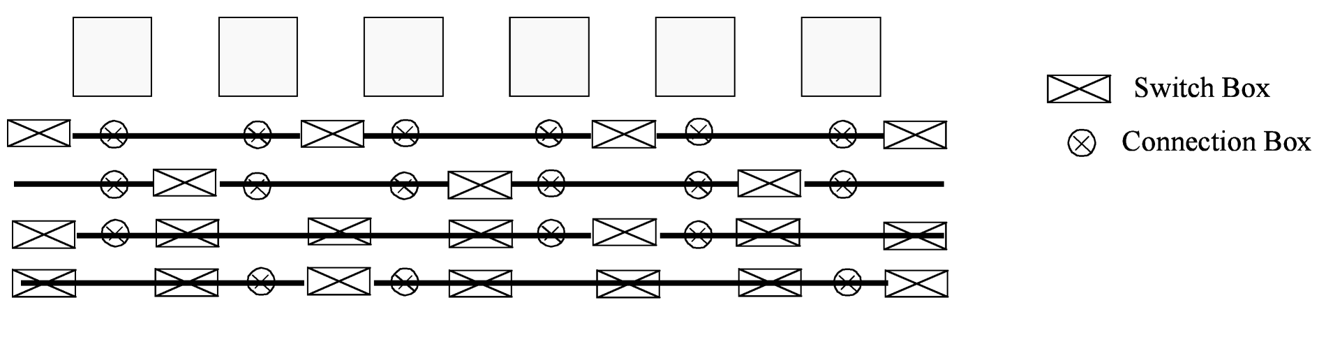
Fig. 35 Switch block and connection block pattern example with four tracks per channel
- <sb type="pattern">int list</sb>intlist" title="Link to this definition">
This tag describes the switch block depopulation (as illustrated in Fig. 35) for this particular wire segment. For example, the first length 6 wire in the figure below has an sb pattern of
1 0 1 0 1 0 1. The second wire has a pattern of0 1 0 1 0 1 0. A1indicates the existence of a switch block and a0indicates that there is no switch box at that point. Note that there are 7 entries in the integer list for a length 6 wire. For a length L wire there must be L+1 entries separated by spaces.Note
Can not be specified for
longlinesegments (which assume full switch block population)Note
This tag may be omitted for segments with
freq="0"(i.e. segments that contribute no tracks to the channel).
- <cb type="pattern">int list</cb>intlist" title="Link to this definition">
This tag describes the connection block depopulation (as illustrated by the circles in Fig. 35) for this particular wire segment. For example, the first length 6 wire in the figure below has an sb pattern of
1 1 1 1 1 1. The third wire has a pattern of1 0 0 1 1 0. A1indicates the existence of a connection block and a0indicates that there is no connection box at that point. Note that there are 6 entries in the integer list for a length 6 wire. For a length L wire there must be L entries separated by spaces.Note
Can not be specified for
longlinesegments (which assume full connection block population)Note
This tag may be omitted for segments with
freq="0"(i.e. segments that contribute no tracks to the channel).
- <mux name="string"/>" title="Link to this definition">
- Required Attributes:
name – Name of the mux switch type used to drive this type of segment by default, from both block outputs and other wires. This information is used during rr-graph construction, and a custom switch block can override this switch type for specific connections if desired. The switch type specified with the <mux> tag will be used for both the incrementing and decrementing wires within this segment. If more control is needed, the mux_inc and mux_dec tags can be used to assign different muxes to drive incremental and decremental wires within the segment.
Note
This tag is only supported for unidirectional routing.
Tag must be included and
namemust be the same as the name you give in<switch type="mux" name="...
- <mux_inc name="string"/>" title="Link to this definition">
- Required Attributes:
name – Name of the mux switch type used to drive the incremental wires in this segment from both block outputs and other wires. Incremental wires are tracks within this segment that are heading in the “right” direction on the x-axis and the “top” direction on the y-axis. This information is used during rr-graph construction, and a custom switch block can override this switch type for specific connections if desired.
Note
This tag is only supported for unidirectional routing.
- <mux_dec name="string">" title="Link to this definition">
- Required Attributes:
name – Name of the mux switch type used to drive the decremental wires in this segment from both block outputs and other wires. Incremental wires are tracks within this segment that are heading in the “left” direction on the x-axis and the “bottom” direction on the y-axis. This information is used during rr-graph construction, and a custom switch block can override this switch type for specific connections if desired.
Note
This tag is only supported for unidirectional routing.
Note
For unidirectional segments, either <mux> tag or both <mux_inc> and <mux_dec> should be defined in the architecture file. If only the <mux> tag is defined, we assume that the same mux drives both incremental and decremental wires within this segment.
- <mux_inter_die name="string"/>" title="Link to this definition">
- Required Attributes:
name – Name of the mux switch type used to drive this segment type when the driver (block outputs and other wires) is located on a different die than the segment. This information is utilized during rr-graph construction.
Tag must be included and
namemust be the same as the name you give in<switch type="mux" name="...
- <wire_switch name="string"/>" title="Link to this definition">
- Required Attributes:
name – Name of the switch type used by other wires to drive this type of segment by default. This information is used during rr-graph construction, and a custom switch block can override this switch type for specific connections if desired.
Tag must be included and the name must be the same as the name you give in
<switch type="tristate|pass_gate" name="...for the switch which represents the wire switch in your architecture.Note
This tag is only supported for bidirectional routing.
- <opin_switch name="string"/>" title="Link to this definition">
- Required Attributes:
name – Name of the switch type used by block pins to drive this type of segment.
Tag must be included and
namemust be the same as the name you give in<switch type="tristate|pass_gate" name="...for the switch which represents the output pin switch in your architecture.Note
This tag is only supported for bidirectional routing.
Clocks
There are two options for describing clocks. One method allows you to specify clocking purely for power estimation, see Specifying Clocking Purely for Power Estimation. The other method allows you to specify a clock architecture that is used as part of the routing resources, see Specifying a Clock Architecture. Both methods should not be used in tandem.
Specifying Clocking Purely for Power Estimation
The clocking configuration is specified with <clock> tags within the <clocks> section.
Note
Currently the information in the <clocks> section is only used for power estimation.
See also
Power Estimation for more details.
- <clock C_wire="float" C_wire_per_m="float" buffer_size={"float"|"auto"}/>" title="Link to this definition">
- Optional Attributes:
C_wire – The absolute capacitance, in Farads, of the wire between each clock buffer.
C_wire_per_m – The wire capacitance, in Farads per Meter.
buffer_size – The size of each clock buffer.
Specifying a Clock Architecture
The element <clocknetworks> contains three sub-elements that collectively describe the clock architecture: the wiring parameters <metal_layers>, the clock distribution <clock_network>, and the clock connectivity <clock_routing>.
Note
The clock network architecture defined in this structure is assigned the fixed default name
"clock_network". When the user wants to specify a net to be routed through the defined clock architecture using a global routing constraints file, the network name attribute in the constraint tag must be set to"clock_network".
Clock Architecture Example
The following example shows how a rib-spine (row/column) style clock architecture can be defined.
<clocknetworks>
    <metal_layers>
        <metal_layer name="global_spine" Rmetal="50.42" Cmetal="20.7e-15"/>
        <metal_layer name="global_rib" Rmetal="50.42" Cmetal="20.7e-15"/>
    </metal_layers>

    <!-- Full Device: Center Spine -->
    <clock_network  name="spine1" num_inst="2">
        <spine metal_layer="global_spine" x="W/2" starty="0" endy="H">
            <switch_point type="drive" name="drive_point" yoffset="H/2" buffer="drive_buff"/>
            <switch_point type="tap" name="taps" yoffset="0" yincr="1"/>
        </spine>
    </clock_network>

    <!-- Full Device: Each Grid Row -->
    <clock_network  name="rib1" num_inst="2">
        <rib metal_layer="global_rib" y="0" startx="0" endx="W" repeatx="W" repeaty="1">
            <switch_point type="drive" name="drive_point" xoffset="W/2" buffer="drive_buff"/>
            <switch_point type="tap" name="taps" xoffset="0" xincr="1"/>
        </rib>
    </clock_network>

    <clock_routing>
        <!-- connections from inter-block routing to central spine -->
        <tap from="ROUTING" to="spine1.drive_point" locationx="W/2" locationy="H/2" switch="general_routing_switch" fc_val="1.0"/>

        <!-- connections from spine to rib -->
        <tap from="spine1.taps" to="rib1.drive_point" switch="general_routing_switch" fc_val="0.5"/>

        <!-- connections from rib to clock pins -->
        <tap from="rib1.taps" to="CLOCK" switch="ipin_cblock" fc_val="1.0"/>
    </clock_routing >
</clocknetworks >

Fig. 36 <spine> “spine1” vertical clock wire example.
The two spines (num_inst="2") are located horizontally at W/2 (in the middle of the device), and spans the entire height of the device (0..H).
The drive points are located at H/2, with tap points located at unit increments along their length.
Buffers of drive_buff type (would be defined in <switches>) are used to drive the two halves of the spines.

Fig. 37 <rib> “rib1” horizontal clock wire example.
Each rib spans the full width of the device (0..W), with the drive points located at the mid-point (W/2), and tap points in unit increments along each rib.
There are two ribs at each vertical location (num_inst="2"), and pairs of ribs are stamped out at each row of the device (repeaty="1").
Power
Additional power options are specified within the <architecture> level <power> section.
See also
See Power Estimation for full documentation on how to perform power estimation.
Direct Inter-block Connections
The content within the <directlist> tag consists of a group of <direct> tags.
The <direct> tag and its contents are described below.
Note
from_pin and to_pin only support big endian! For example, clb.out[8:0]
- <direct name="string" from_pin="string" to_pin="string" x_offset="int" y_offset="int" z_offset="int" switch_name="string" from_side="{left|right|top|bottom}" to_side="{left|right|top|bottom}"/>" title="Link to this definition">
- Required Attributes:
name – is a unique alphanumeric string to name the connection.
from_pin – pin of complex block that drives the connection.
to_pin – pin of complex block that receives the connection.
x_offset – The x location of the receiving complex block relative to the driving complex block.
y_offset – The y location of the receiving complex block relative to the driving complex block.
z_offset – The z location of the receiving complex block relative to the driving complex block.
- Optional Attributes:
switch_name – The name of the
<switch>from<switchlist>to be used for this direct connection. Default: switch with zero delay (i.e., short)from_side – The associated from_pin’s block side
to_side – The associated to_pin’s block side
Describes a dedicated connection between two complex block pins that skips general interconnect. This is useful for describing structures such as carry chains as well as adjacent neighbour connections.
The
from_sideandto_sideoptions can usually be left unspecified. However they can be used to explicitly control how direct connections to physically equivalent pins (which may appear on multiple sides) are handled.
Example: Inter-tile connection
Consider a carry chain where the cout of each CLB drives the cin of the CLB immediately below it, using the delay-less switch one would enter the following:
<direct name="adder_carry" from_pin="clb.cout" to_pin="clb.cin" x_offset="0" y_offset="-1" z_offset="0"/>
Example: Inner-tile feedback
Consider a feedback connection where the out of each CLB drives the in of the CLB in the same location, using the connection block switch one would enter the following:
<direct name="feedback" from_pin="clb.out" to_pin="clb.in" x_offset="0" y_offset="0" z_offset="0" switch_name="cb_mux"/>
Example: Cross-sub-tile connection
In this example, a tile cim8_1k is defined, under which there are two types of sub-tiles:
mult_8: the first sub-tilememory: the second, and the third sub-tile
<tile name="cim8_1k" height="2" area="396000">
  <sub_tile name="mult_8" capacity="1">
    <equivalent_sites>
      <site pb_type="mult_8" pin_mapping="direct"/>
    </equivalent_sites>
    <input name="a" num_pins="8"/>
    <input name="b" num_pins="8"/>
    <output name="out" num_pins="16"/>
    <fc in_type="frac" in_val="0.15" out_type="frac" out_val="0.10">
      <fc_override port_name="out" fc_type="frac" fc_val="0"/>
    </fc>
    <pinlocations pattern="custom">
      <loc side="left"/>
      <loc side="top"/>
      <loc side="right" yoffset="0">mult_8.a[0:2] mult_8.b[0:2] mult_8.out[0:5]</loc>
      <loc side="right" yoffset="1">mult_8.a[3:5] mult_8.b[3:5] mult_8.out[6:10]</loc>
      <loc side="bottom">mult_8.a[6:7] mult_8.b[6:7] mult_8.out[11:15]</loc>
    </pinlocations>
  </sub_tile>
  <sub_tile name="memory" capacity="2">
    <equivalent_sites>
      <site pb_type="memory"/>
    </equivalent_sites>
    <input name="waddr" num_pins="7"/>
    <input name="raddr" num_pins="7"/>
    <input name="data_in" num_pins="8"/>
    <input name="wen" num_pins="1"/>
    <input name="ren" num_pins="1"/>
    <output name="data_out" num_pins="8"/>
    <clock name="clk" num_pins="1"/>
    <fc in_type="frac" in_val="0.15" out_type="frac" out_val="0.10">
      <fc_override port_name="clk" fc_type="frac" fc_val="0"/>
      <fc_override port_name="data_in" fc_type="frac" fc_val="0"/>
    </fc>
    <pinlocations pattern="custom">
      <loc side="left" yoffset="0">memory.clk memory.waddr[0:0] memory.raddr[0:0] memory.data_in[0:0] memory.data_out[0:0]</loc>
      <loc side="left" yoffset="1">memory.waddr[1:1] memory.raddr[1:1] memory.data_in[1:1] memory.data_out[1:1]</loc>
      <loc side="top" yoffset="1">memory.waddr[2:2] memory.raddr[2:2] memory.data_in[2:2] memory.data_out[2:2] memory.waddr[3:3] memory.raddr[3:3] memory.data_in[3:3] memory.data_out[3:3]</loc>
      <loc side="right" yoffset="0">memory.waddr[4:4] memory.raddr[4:4] memory.data_in[4:4] memory.data_out[4:4]</loc>
      <loc side="right" yoffset="1">memory.waddr[5:5] memory.raddr[5:5] memory.data_in[5:5] memory.data_out[5:5]</loc>
      <loc side="bottom" yoffset="0">memory.wen memory.waddr[6:6] memory.raddr[6:6] memory.data_in[6:6] memory.data_out[6:6] memory.ren memory.data_in[7:7] memory.data_out[7:7]</loc>
    </pinlocations>
  </sub_tile>
</tile>
As shown in Fig. 38, consider a connection where the out of a sub tile mult_8 of tile cim8_1k drives the data_in of the sub tile memory of tile cim8_1k with an offset, using the delayless switch one would enter the following:
<direct name="cim_direct0" from_pin="cim8_1k.out[7:0]" to_pin="cim8_1k.data_in[7:0]" x_offset="0" y_offset="0" z_offset="1"/>
<direct name="cim_direct1" from_pin="cim8_1k.out[15:8]" to_pin="cim8_1k.data_in[7:0]" x_offset="0" y_offset="0" z_offset="2"/>
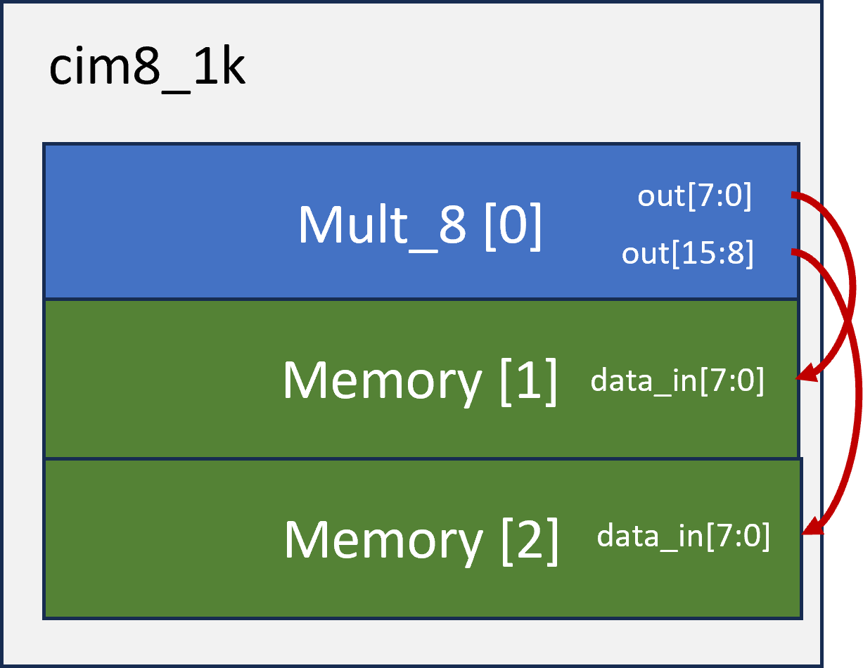
Fig. 38 Example of direct connections across sub-tiles
Custom Switch Blocks
The content under the <switchblocklist> tag consists of one or more <switchblock> tags that are used to specify connections between different segment types. An example is shown below:
<switchblocklist>
  <switchblock name="my_switchblock" type="unidir">
    <switchblock_location type="EVERYWHERE"/>
    <switchfuncs>
      <func type="lr" formula="t"/>
      <func type="lt" formula="W-t"/>
      <func type="lb" formula="W+t-1"/>
      <func type="rt" formula="W+t-1"/>
      <func type="br" formula="W-t-2"/>
      <func type="bt" formula="t"/>
      <func type="rl" formula="t"/>
      <func type="tl" formula="W-t"/>
      <func type="bl" formula="W+t-1"/>
      <func type="tr" formula="W+t-1"/>
      <func type="rb" formula="W-t-2"/>
      <func type="tb" formula="t"/>
    </switchfuncs>
    <wireconn from_type="l4" to_type="l4" from_switchpoint="0,1,2,3" to_switchpoint="0"/>
    <wireconn from_type="l8_global" to_type="l8_global" from_switchpoint="0,4"
          to_switchpoint="0"/>
    <wireconn from_type="l8_global" to_type="l4" from_switchpoint="0,4"
          to_switchpoint="0"/>
  </switchblock>

  <switchblock name="another_switch_block" type="unidir">
    ... another switch block description ...
  </switchblock>
</switchblocklist>
This switch block format allows a user to specify mathematical permutation functions that describe how different types of segments (defined in the architecture file under the <segmentlist> tag) will connect to each other at different switch points.
The concept of a switch point is illustrated below for a length-4 unidirectional wire heading in the “left” direction.
The switch point at the start of the wire is given an index of 0 and is incremented by 1 at each subsequent switch block until the last switch point.
The last switch point has an index of 0 because it is shared between the end of the current segment and the start of the next one (similarly to how switch point 3 is shared by the two wire subsegments on each side).
Fig. 39 Switch point diagram.
A collection of wire types and switch points defines a set of wires which will be connected to another set of wires with the specified permutation functions (the ‘sets’ of wires are defined using the <wireconn> tags).
This format allows for an abstract but very flexible way of specifying different switch block patterns.
For additional discussion on interconnect modeling see [Pet16].
The full format is documented below.
Overall Notes:
The
<sb type="pattern">tag on a wire segment (described under<segmentlist>) is applied as a mask on the patterns created by this switch block format; anywhere along a wire’s length where a switch block has not been requested (set to 0 in this tag), no switches will be added.You can specify multiple switchblock tags, and the switches described by the union of all those switch blocks will be created.
- <switchblock name="string" type="string">" title="Link to this definition">
- Required Attributes:
name – A unique alphanumeric string
type –
unidirorbidir. A bidirectional switch block will implicitly mirror the specified permutation functions – e.g. if a permutation function of typelr(function used to connect wires from the left to the right side of a switch block) has been specified, a reverse permutation function of typerl(right-to-left) is automatically assumed. A unidirectional switch block makes no such implicit assumptions. The type of switch block must match the directionality of the segments defined under the<segmentlist>node.
<switchblock>is the top-level XML node used to describe connections between different segment types.Each
<switchblock>must contain exactly one<switchblock_location>tag and exactly one<switchfuncs>tag.
- <switchblock_location type="string"/>" title="Link to this definition">
- Required:
Yes
- Required Attributes:
type –
Can be one of the following strings:
EVERYWHERE– at each switch block of the FPGAPERIMETER– at each perimeter switch block (x-directed and/or y-directed channel segments may terminate here)CORNER– only at the corner switch blocks (both x and y-directed channels terminate here)FRINGE– same as PERIMETER but excludes cornersCORE– everywhere but the perimeterXY_SPECIFIED– only at one or more explicitly specified grid locations, rows/columns, or regions
Sets the location on the FPGA where the connections described by this switch block will be instantiated.
Explicitly specified locations (
type="XY_SPECIFIED")When the type is
XY_SPECIFIED, the switch block is instantiated only at the grid locations selected by the additional coordinate attributes. All coordinate attributes are evaluated as formulas which may reference the variablesWandH, denoting the device grid width and height respectively (e.g.endx="W-1").Note
XY_SPECIFIEDrequires a fixed device layout (a named<fixed_layout>); it is not supported with anautolayout, since the grid dimensions must be known when the architecture is parsed.There are three ways to select locations:
A single switch block – specify both
xandy. The switch block is created only at grid location(x, y).An entire row or column – specify one coordinate and set the other to
-1for the entire row or column.x="C" y="-1"applies the switch block to the entire column atx = C(all rows).x="-1" y="R"applies the switch block to the entire row aty = R(all columns).
A region – specify one rectangular region (optionally repeating) with the attributes below.
- Optional Attributes:
startx – X coordinate of the first column of the region. Default:
0.endx – X coordinate of the last column of the region. Default:
W-1.starty – Y coordinate of the first row of the region. Default:
0.endy – Y coordinate of the last row of the region. Default:
H-1.repeatx – Horizontal repeat factor at which the region repeats across the grid. Default:
0(the region does not repeat).repeaty – Vertical repeat factor at which the region repeats across the grid. Default:
0(the region does not repeat).incrx – Horizontal stride within the region; only every
incrx-th column of the region receives the switch block. Default:1.incry – Vertical stride within the region; only every
incry-th row of the region receives the switch block. Default:1.
Note
If either
xoryis specified (i.e. not-1), the region attributes are ignored.The following examples all use
type="XY_SPECIFIED":<!-- A single switch block at grid location (4, 7) --> <switchblock_location type="XY_SPECIFIED" x="4" y="7"/> <!-- The entire column at x = 1 (all rows) --> <switchblock_location type="XY_SPECIFIED" x="1" y="-1"/> <!-- The entire row at y = 1 (all columns) --> <switchblock_location type="XY_SPECIFIED" x="-1" y="1"/> <!-- Columns 2, 5, 8, ... (a one-column-wide region repeating every 3 columns), for all rows --> <switchblock_location type="XY_SPECIFIED" startx="2" endx="2" repeatx="3"/>
- <switchfuncs>
- Required:
Yes
The switchfuncs XML node contains one or more
<func>entries that specify the permutation functions with which different switch block sides should be connected, as described below. At least one<func>entry must be present.
- <func type="string" formula="string"/>" title="Link to this definition">
- Required Attributes:
type –
Specifies which switch block sides this function should connect. With the switch block sides being left, top, right and bottom, the allowed entries are one of {
lt,lr,lb,tr,tb,tl,rb,rl,rt,bl,bt,br} whereltmeans that the specified permutation formula will be used to connect the left-top sides of the switch block.Note
In a bidirectional architecture the reverse connection is implicit.
formula –
Specifies the mathematical permutation function that determines the pattern with which the source/destination sets of wires (defined using the <wireconn> entries) at the two switch block sides will be connected. For example,
W-tspecifies a connection where thet’th wire in the source set will connect to theW-twire in the destination set whereWis the number of wires in the destination set and the formula is implicitly treated as moduloW.Special characters that can be used in a formula are:
t– the index of a wire in the source setW– the number of wires in the destination set (which is not necessarily the total number of wires in the channel)
The operators that can be used in the formula are:
Addition (
+)Subtraction (
-)Multiplication (
*)Division (
/)Brackets
(and)are allowed and spaces are ignored.
Defined under the
<switchfuncs>XML node, one or more<func...>entries is used to specify permutation functions that connect different sides of a switch block.
- <wireconn num_conns="expr" from_type="string, string, string, ..." to_type="string, string, string, ..." from_switchpoint="int, int, int, ..." to_switchpoint="int, int, int, ..." from_order="{fixed | shuffled}" to_order="{fixed | shuffled}" switch_override="string" side="string"/>" title="Link to this definition">
- Required Attributes:
num_conns –
Specifies how many connections should be created between the from_type/from_switchpoint set and the to_type/to_switchpoint set. The value of this parameter is an expression which is evaluated when the switch block is constructed.
The expression can be a single number or formula using the variables:
from– The number of switchblock edges equal to the ‘from’ set size.This ensures that each element in the ‘from’ set is connected to an element of the ‘to’ set. However it may leave some elements of the ‘to’ set either multiply-connected or disconnected.

to– The number of switchblock edges equal to the ‘to’ set size.This ensures that each element of the ‘to’ set is connected to precisely one element of the ‘from’ set. However it may leave some elements of the ‘from’ set either multiply-connected or disconnected.

Examples:
min(from,to)– Creates number of switchblock edges equal to the minimum of the ‘from’ and ‘to’ set sizes.This ensures no element of the ‘from’ or ‘to’ sets is connected to multiple elements in the opposing set. However it may leave some elements in the larger set disconnected.

max(from,to)– Creates number of switchblock edges equal to the maximum of the ‘from’ and ‘to’ set sizes.This ensures all elements of the ‘from’ or ‘to’ sets are connected to at least one element in the opposing set. However some elements in the smaller set may be multiply-connected.

3*to– Creates number of switchblock edges equal to three times the ‘to’ set sizes.
from_type – A comma-separated list of segment names that defines which segment types will be a source of a connection. The segment names specified must match the names of the segments defined under the
<segmentlist>XML node. When multiple segment types are listed, each type shares the samefrom_switchpointvalues, and the overall source set is the union of all (type, switchpoint) pairs. Required if no<from>or<to>nodes are specified within the<wireconn>.to_type – A comma-separated list of segment names that defines which segment types will be the destination of the connections specified. Each segment name must match an entry in the
<segmentlist>XML node. When multiple segment types are listed, each type shares the sameto_switchpointvalues, and the overall destination set is the union of all (type, switchpoint) pairs. Required if no<from>or<to>nodes are specified within the<wireconn>.from_switchpoint – A comma-separated list of integers that defines which switchpoints will be a source of a connection. Required if no
<from>or<to>nodes are specified within the<wireconn>.to_switchpoint –
A comma-separated list of integers that defines which switchpoints will be the destination of the connections specified. Required if no
<from>or<to>nodes are specified within the<wireconn>.Note
In a unidirectional architecture wires can only be driven at their start point so
to_switchpoint="0"is the only legal specification in this case.
- Optional Attributes:
from_order –
Specifies the order in which
from_switchpoints are selected when creating edges.fixed– Switchpoints are selected in the order specifiedThis is useful to specify a preference for connecting to specific switchpoints. For example,
<wireconn num_conns="1*to" from_type="L16" from_switchpoint="0,12,8,4" from_order="fixed" to_type="L4" to_switchpoint="0"/>
specifies L4 wires should be connected first to L16 at switchpoint 0, then at switchpoints 12, 8, and 4. This is primarily useful when we want to ensure that some switchpoints are ‘used-up’ first.
shuffled– Switchpoints are selected in a (randomly) shuffled orderThis is useful to ensure a diverse set of switchpoints are used. For example,
<wireconn num_conns="1*to" from_type="L4" from_switchpoint="0,1,2,3" from_order="shuffled" to_type="L4" to_switchpoint="0"/>
specifies L4 wires should be connected to other L4 wires at any of switchpoints 0, 1, 2, or 3. Shuffling the switchpoints is useful if one of the sets (e.g. from L4’s) is much larger than the other (e.g. to L4’s), and we wish to ensure a variety of switchpoints from the larger set are used.
Default:
shuffledto_order –
Specifies the order in which ``to_switchpoint``s are selected when creating edges.
Note
See
from_orderfor value descriptions.Default:
shuffledswitch_override –
Specifies the name of a switch to be used to override the wire_switch of the segments in the
toset. Can be used to create switch patterns where different switches are used for different types of connections. By using a zero-delay and zero-resistance switch one can also create T and L shaped wire segments.Default: If no override is specified, the usual wire_switch that drives the
towire will be used.side – Specifies the sides that connections are gathered from or scattered to. Valid sides are right, left, top and bottom and are represented by characters ‘r’, ‘l’, ‘t’ and ‘b’. For example, to select connections from right, left and bottom set this attribute to “rlb”. Note that this attribute is used only for Scatter-Gather Patterns and does not do anything for other usages of this tag.
- <from type="string" switchpoint="int, int, int, ..."/>" title="Link to this definition">
- Required Attributes:
type – The name of a segment specified in the
<segmentlist>.switchpoint –
A comma-separated list of integers that defines switchpoints.
Note
In a unidirectional architecture wires can only be driven at their start point so
to_switchpoint="0"is the only legal specification in this case.
Specifies a subset of source wire switchpoints.
This tag can be specified multiple times. The surrounding
<wireconn>’s source set is the union of all contained<from>tags.Note
<from>sub-tags and thefrom_type/from_switchpointattributes are mutually exclusive on a given<wireconn>. If<from>sub-tags are present, thefrom_typeandfrom_switchpointattributes are ignored. Use sub-tags when you need to specify different switchpoints for different segment types; use attributes when all types share the same switchpoints.
- <to type="string" switchpoint="int, int, int, ..."/>" title="Link to this definition">
Specifies a subset of destination wire switchpoints.
This tag can be specified multiple times. The surrounding
<wireconn>’s destination set is the union of all contained<to>tags.Note
<to>sub-tags and theto_type/to_switchpointattributes are mutually exclusive on a given<wireconn>. If<to>sub-tags are present, theto_typeandto_switchpointattributes are ignored.See also
<from>for attribute descriptions.
As an example, consider the following
<wireconn>specification:<wireconn num_conns_type="to"/> <from type="L4" switchpoint="0,1,2,3"/> <from type="L16" switchpoint="0,4,8,12"/> <to type="L4" switchpoint="0/> </wireconn>
This specifies that the ‘from’ set is the union of L4 switchpoints 0, 1, 2 and 3; and L16 switchpoints 0, 4, 8 and 12. The ‘to’ set is all L4 switchpoint 0’s. Note that since different switchpoints are selected from different segment types it is not possible to specify this without using
<from>sub-tags.
Scatter-Gather Patterns
The content under the <scatter_gather_list> tag consists of one or more <sg_pattern> tags that are used to specify a scatter-gather pattern.
Scatter-gather patterns can be used to specify multi-level switch patterns, rather than the direct wire-to-wire switch patterns of conventional switch blocks.
These additional switches, wires and/or muxes will be added to the architecture, augmenting wires created using segment specifications and switches created using switch box specifications.
The number of additional wires or muxes created by scatter-gather specifications may be fixed or given by a formula in the routing channel width W (e.g. in <sg_location> or <interdie_wire> num attributes).

Fig. 40 Overview of how scatter-gather patterns work. First, connections from a switchblock location are selected according to the specification. These selected connection are then muxed and passed through the scatter-gather node, which is typically a wire segment. The scatter-gather node then fans out or scatters in another switchblock location.
When instantiated, a scatter-gather pattern gathers connections from a switchblock and passes the connection through a multiplexer and the scatter-gather node which is typically a wire segment, then scatters or fans out somewhere else in the device. These patterns can be used to define 3D switchblocks.
Note
For inter-layer scatter-gather links (z_offset != 0), VPR skips instantiation when either the gather or scatter endpoint has a short switchblock type (horizontal_short, vertical_short, or straight_short).
This models regions such as TSV holes reserved for power delivery, where inter-layer connectivity is not feasible.
As a result, some scatter-gather links specified by <sg_location> tags are ignored at those grid locations even though they match the specified region.
An example is shown below:
<scatter_gather_list>
    <sg_pattern name="name" type="unidir">
        <gather>
            <!-- Gather 30 connections from the 0, 4, 8 or 12 position of L16 wires of all four sides of a switchblock location -->
            <wireconn num_conns="30" from_type="L16" from_switchpoint="0,12,8,4" side="rltb"/>
        <gather/>

        <scatter>
            <!-- Scatter 30 connections to the starting position of L16 wires of all four sides of a switchblock location -->
            <wireconn num_conns="30" to_type="L16" to_switchpoint="0" side="rtlb"/>
        <scatter/>

        <sg_link_list>
            <!-- Link going up one layer, using the '3D_SB_MUX' multiplexer to gather connections from the bottom layer and using the 'TSV' node/wire to move up one layer -->
            <sg_link name="L_UP" z_offset="1" x_offset="0" y_offset="0" mux="3D_SB_MUX" seg_type="TSV"/>
            <!-- Same as above but moving one layer down -->
            <sg_link name="L_DOWN" z_offset="-1" mux="3D_SB_MUX" seg_type="TSV"/>
        <sg_link_list/>

        <!-- Instantiate 10 'L_UP' sg_links per switchblock location everywhere on the device -->
        <sg_location type="EVERYWHERE" num="10" sg_link="L_UP"/>
        <!-- Instantiate 10 'L_DOWN' sg_links per switchblock location everywhere on the device -->
        <sg_location type="EVERYWHERE" num="10" sg_link="L_DOWN"/>
    <sg_pattern/>

    <sg_pattern name="interposer_conn_sg" type="bidir">
        ... <!-- Another scatter-gather pattern specification -->
    <sg_pattern/>
<scatter_gather_list/>
- <sg_pattern name="string" type={unidir|bidir}>" title="Link to this definition">
- Required Attributes:
name – A unique alphanumeric string
type –
Directionality of the scatter-gather connection
unidir: Added connections are unidirectional; all the gather connections are combined in a mux that then drives the scatter-gather node which in turn drives the wires specified in the scatter specification.bidir: The gather and scatter connections are mirrored; the same scatter pattern is implemented at each end of the scatter-gather pattern. This implies the two muxes driving the scatter-gather node can have their outputs tri-state buffered.
- <gather>
Contains a
<wireconn>tag specifying how the fan-in or gather connections are selected. Seewireconnfor the relevant specification. This<wireconn>tag supports an additioinalsideattribute which selects the sides that connections are gathered from (e.g.side="rltb"means that connections are gathered from the right, left, top, and bottom sides of the switch block).
- <scatter>
Contains a
<wireconn>tag specifying how the fan-out or scatter connections are selected. Seewireconnfor the relevant specification. This<wireconn>tag supports an additioinalsideattribute which selects the sides that connections are scattered to (e.g.side="rltb"means that connections are scattered to the right, left, top, and bottom sides of the switch block).
- <sg_link_list>
Contains one or more
<sg_link>tags specifying how the gather and scatter locations are connected (i.e. defines the used mux and scatter-gather node).Note
<sg_link>tags are not instantiations of the pattern and would not result in any changes to the device. Instead, the<sg_location>tag instantiates the pattern and selects one of the<sg_link>tags to be used for the instantiation.
- <sg_link name="string" x_offset="int" y_offset="int" z_offset="int" mux="string" seg_type="string">" title="Link to this definition">
- Required Attributes:
name – A unique alphanumeric string
mux – Name of the multiplexer used to gather connections
seg_type – Name of the segment used to connect the gather and scatter locations (i.e. the type of the scatter-gather node)
- Optional Attributes:
x_offset – Offset of the scatter relative to the gather in the x-axis
y_offset – Offset of the scatter relative to the gather in the y-axis
z_offset – Offset of the scatter relative to the gather in the z-axis
Note
Only one of the offset fields for the sg_link tag should be set. The magnitude of the offset will generally be chosen by the architecture file creator to match the length of the sg_link segment type.
- <sg_location type="string" num="expr" sg_link_name="string">" title="Link to this definition">
Instantiates the scatter-gather pattern with the specified sg_link.
- Required Attributes:
num – Number of scatter-gather instances per matching location (e.g. per switch block). May be an integer or a formula; the variable
Wdenotes the routing channel width when the expression is evaluated.sg_link_name – Name of the
sg_linkused in the instantiationtype – Can be one of the following strings: *
EVERYWHERE– at each switch block of the FPGA *PERIMETER– at each perimeter switch block (x-directed and/or y-directed channel segments may terminate here) *CORNER– only at the corner switch blocks (both x and y-directed channels terminate here) *FRINGE– same as PERIMETER but excludes corners *CORE– everywhere but the perimeter
Sets the location on the FPGA where the connections described by this scatter-gather pattern be instantiated.
Architecture metadata
Architecture metadata enables tagging of architecture or routing graph information that exists outside of the normal VPR flow (e.g. pack, place, route, etc). For example this could be used to enable bitstream generation by tagging routing edges and pb_type features.
The metadata will not be used by the vpr executable, but can be leveraged by new tools using the libvpr library. These new tools can access the metadata on the various VPR internal data structures.
To enable tagging of architecture structures with metadata, the <metadata>
tag can be inserted under the following XML tags:
<pb_type>Any tag under
<interconnect>(<direct>,<mux>, etc).<mode>Any grid location type (
<perimeter>,<fill>,<corners>,<single>,<col>,<row>,<region>)
- <metadata>
Specifies the root of a metadata block. Can have 0 or more <meta> Children.
- <meta name="string" >" title="Link to this definition">
- Required Attributes:
name – Key name of this metadata value.
Specifies a value within a metadata block. The name is a key
for looking up the value contained within the <meta> tag. Keys can be
repeated, and will be stored in a vector in order of occurrence.
The value of the <meta> is the text in the block. Both the name and
<meta> value will be stored as a string. XML children are not supported
in the <meta> tag.
Example of a metadata block with 2 keys:
<metadata>
  <meta name="some_key">Some value</meta>
  <meta name="other key!">Other value!</meta>
</metadata>
Additional Syntax for Tileable Architecture
When tileable architecture is enabled, the following options are available in the architecture file:
Layout
<layout> may include additioinal attributes to enable tileable routing resource graph generation
- tileable="<bool>"
Turn
on/offthe tileable routing resource graph generator.The tileable routing architecture can minimize the number of unique modules in FPGA fabric to be physically implemented.
Technical details can be found in [TGAG19].
Note
It is strongly recommended to enable the tileable routing architecture when you want to PnR large FPGA fabrics, which can effectively reduce the runtime.
- through_channel="<bool>"
Allow routing channels to pass through multi-width and multi-height programmable blocks. This is mainly used in heterogeneous FPGAs to increase routability, as illustrated in Fig. 41. By default, it is
false.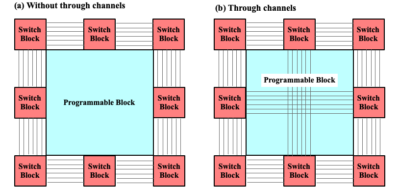
Fig. 41 Impact on routing architecture when through channel in multi-width and multi-height programmable blocks: (a) disabled; (b) enabled.
Warning
Do NOT enable
through_channelif you are not using the tileable routing resource graph generator!Warning
You cannot use
spreadpin location for theheight > 1orwidth >1tiles when using the tileable routing resource graph. Otherwise, it will cause undriven pins in your device!!!
- shrink_boundary="<bool>"
Remove all the routing wires in empty regions. This is mainly used in non-rectangular FPGAs to avoid redundant routing wires in blank area, as illustrated in Fig. 42. By default, it is
false.
Fig. 42 Impact on routing architecture when shrink-boundary: (a) disabled; (b) enabled.
Warning
Do NOT enable
shrink_boundaryif you are not using the tileable routing resource graph generator!
- perimeter_cb="<bool>"
Allow connection blocks to appear around the blocks on the perimeter of the device (mainly I/Os). This is designed to enhance routability of I/Os on perimeter. It is also strongly recommended when a programmable clock network is required to touch clock pins on I/Os. As illustrated in Fig. 43, routing tracks can access three sides of each I/O when perimeter connection blocks are created.
Default:
false
Warning
When enabled, please only place outputs at one side of I/Os. For example, outputs of an I/O on the top side can only occur on the bottom side of the I/O tile. Otherwise, routability loss may be expected, leading to some pins being unreachable. Enable the opin2all_sides to recover routability loss.
Fig. 43 Impact on routing architecture when perimeter connection blocks are : (a) disabled; (b) enabled.
Warning
Do NOT enable perimeter_cb if you are not using the tileable routing resource graph generator!
- opin2all_sides="<bool>"
Allow each output pin of a programmable block to drive the routing tracks on all the sides of its adjacent switch block (see an illustrative example in Fig. 44). This can improve the routability of an FPGA fabric with an increase in the sizes of routing multiplexers in each switch block.
Default:
false
Fig. 44 Impact on routing architecture when the opin-to-all-sides: (a) disabled; (b) enabled.
Warning
Do NOT enable
opin2all_sidesif you are not using the tileable routing resource graph generator!
- concat_wire="<bool>"
In each switch block, allow each routing track which ends to drive another routing track on the opposite side, as such a wire can be continued in the same direction (see an illustrative example in
fig_concat_wire). In other words, routing wires can be concatenated in the same direction across an FPGA fabric. This can improve the routability of an FPGA fabric with an increase in the sizes of routing multiplexers in each switch block.Default:
false
Fig. 45 Impact on routing architecture when the wire concatenation: (a) disabled; (b) enabled.
Warning
Do NOT enable
concat_wireif you are not using the tileable routing resource graph generator!
- concat_pass_wire="<bool>"
In each switch block, allow each routing track which passes to drive another routing track on the opposite side, as such a pass wire can be continued in the same direction (see an illustrative example in
fig_concat_pass_wire). This can improve the routability of an FPGA fabric with an increase in the sizes of routing multiplexers in each switch block.Default:
false
Fig. 46 Impact on routing architecture when the pass wire concatenation: (a) disabled; (b) enabled.
Warning
Do NOT enable
concat_pass_wireif you are not using the tileable routing resource graph generator!
A quick example to show tileable routing is enabled, other options, e.g., through channels are disabled:
<layout tileable="true" through_channel="false" shrink_boundary="false" opin2all_sides="false" concat_wire="false" concat_pass_wire="false">
</layout>
Switch Block
<switch_block> may include addition syntax to enable different connectivity for pass tracks
- sub_type="<string>"
Connecting type for pass tracks in each switch block. The supported connecting patterns are
subset,universalandwilton, being the same as the capability of VPR. If not specified, the pass tracks will have the same connecting patterns as start/end tracks, which are defined intype
- sub_Fs="<int>"
Connectivity parameter for pass tracks in each switch block. Must be a multiple of 3. If not specified, the pass tracks will have the same connectivity as start/end tracks, which are defined in
fs.
- A quick example which defines a switch block
Starting/ending routing tracks are connected in the
wiltonpatternEach starting/ending routing track can drive 3 other starting/ending routing tracks
Passing routing tracks are connected in the
subsetpatternEach passing routing track can drive 6 other starting/ending routing tracks
<device>
  <switch_block type="wilton" fs="3" sub_type="subset" sub_fs="6"/>
</device>
Routing Segments
When using tileable architecture, it is strongly recommended to give explicit names
for each routing segment in <segmentlist>.
This is used to link circuit_model to routing segments.
A quick example which defines a length-4 uni-directional routing segment called L4 :
<segmentlist>
  <segment name="L4" freq="1" length="4" type="undir"/>
</segmentlist>
Note
Currently, tileable architecture only supports uni-directional routing architectures.
Direct Interconnect
This section introduces extensions on the architecture description file about direct connections between programmable blocks.
Syntax
The original direct connections in the directlist section are documented in Direct Inter-block Connections. Its description is given below:
<directlist>
  <direct name="string" from_pin="string" to_pin="string" x_offset="int" y_offset="int" z_offset="int" switch_name="string"/>
</directlist>
Note
These options are required
In the tileable architecture file, you may define additional attributes for each VPR’s direct connection:
<direct_connection>
  <direct name="string" circuit_model_name="string" interconnection_type="string" x_dir="string" y_dir="string"/>
</directlist>
Note
these options are optional. However, if interconnection_type is set to inter_column or inter_row, then x_dir and y_dir are required.
- interconnection_type="<string>"
Available types are
inner_column_or_row|part_of_cb|inter_column|inter_rowinner_column_or_rowindicates the direct connections are between tiles in the same column or row. This is the default value.part_of_cbindicates the direct connections will drive routing multiplexers in connection blocks. Therefore, it is no longer a strict point-to-point direct connection.inter_columnindicates the direct connections are between tiles in two columnsinter_rowindicates the direct connections are between tiles in two rows
Note
The following syntax is only applicable to inter_column and inter_row
- x_dir="<string>"
Available directionalities are
positive|negative, specifies if the next cell to connect has a bigger or lowerxvalue. Considering a coordinate system where (0,0) is the origin at the bottom left andxandyare positives:x_dir=”positive”:
interconnection_type=”inter_column”: a column will be connected to a column on the
right, if it exists.interconnection_type=”inter_row”: the most on the
rightcell from a row connection will connect the most on theleftcell of next row, if it exists.
x_dir=”negative”:
interconnection_type=”inter_column”: a column will be connected to a column on the
left, if it exists.interconnection_type=”inter_row”: the most on the
leftcell from a row connection will connect the most on therightcell of next row, if it exists.
- y_dir="<string>"
Available directionalities are
positive|negative, specifies if the next cell to connect has a bigger or lower x value. Considering a coordinate system where (0,0) is the origin at the bottom left and x and y are positives:y_dir=”positive”:
interconnection_type=”inter_column”: the
bottomcell of a column will be connected to the next columntopcell, if it exists.interconnection_type=”inter_row”: a row will be connected on an
aboverow, if it exists.
y_dir=”negative”:
interconnection_type=”inter_column”: the
topcell of a column will be connected to the next columnbottomcell, if it exists.interconnection_type=”inter_row”: a row will be connected on a row
below, if it exists.
Enhanced Connection Block
A direct connection can also drive routing multiplexers of connection blocks. When such connection occurs in a connection block, it is called an enhanced connection block. Fig. 47 illustrates the difference between a regular connection block and an enhanced connection block.
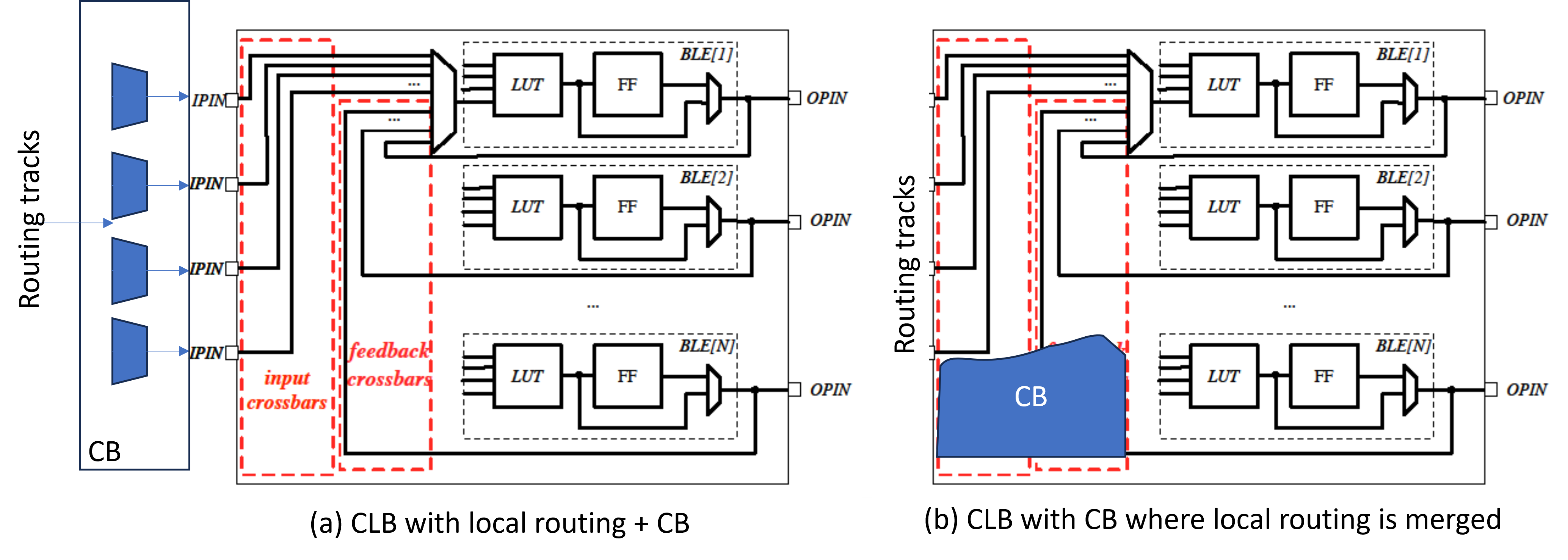
Fig. 47 Enhanced connection block vs. Regular connection block
In such scenario, the type part_of_cb is required.
Warning
Restrictions may be applied when building the direct connections as part of a connection block.
Direct connections can be inside a tile or across two tiles. Currently, across more than two tiles are not supported! Fig. 48 illustrates the region (in red) where any input pin is allowed to be driven by any output pin.
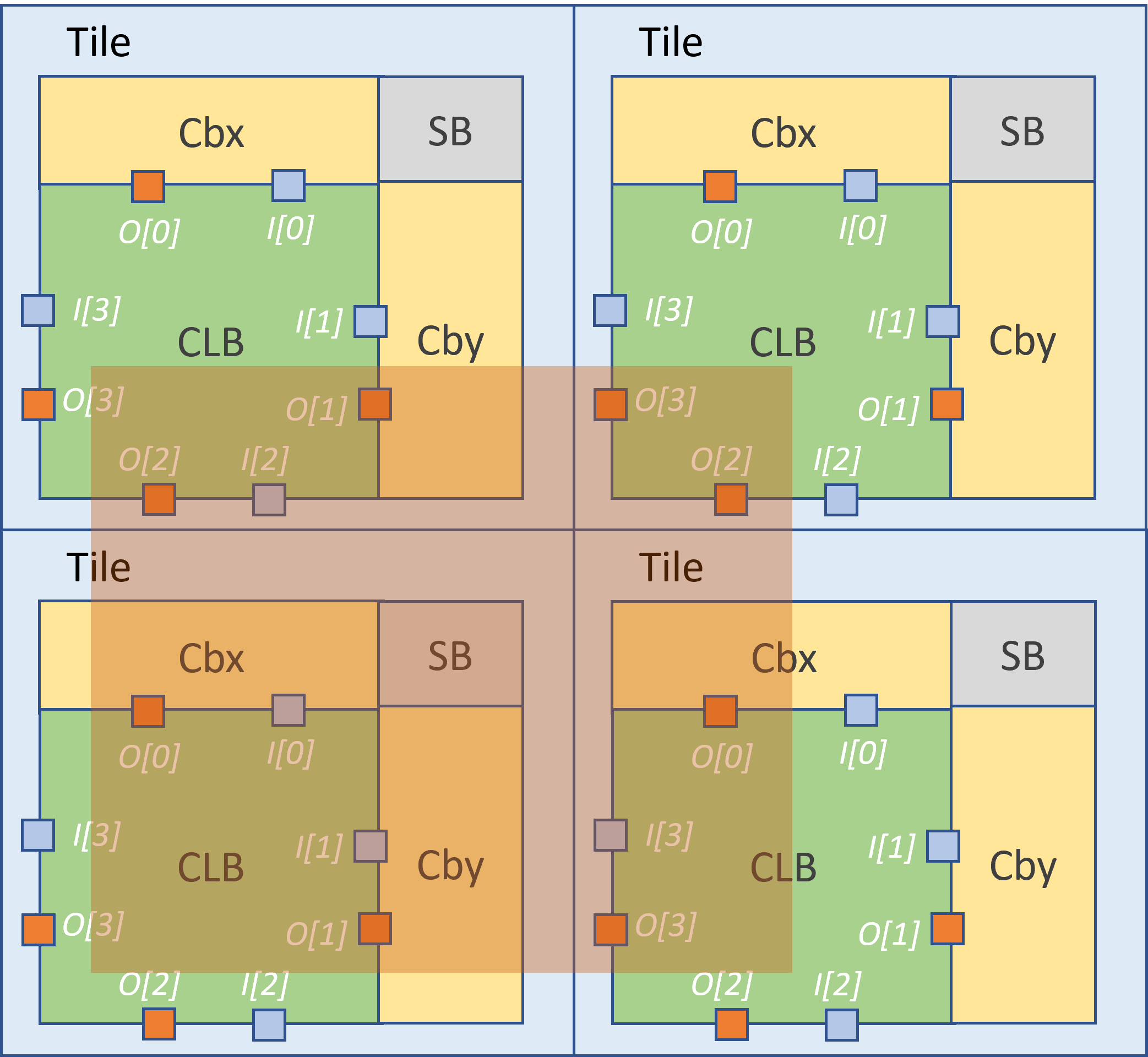
Fig. 48 Allowed connections inside a tile for enhanced connection block (see the highlighted region)
Fig. 49 shows a few feedback connections which can be built inside connection blocks. Note that feedback connections are fully allowed between any pins on the same side of a programmable block.
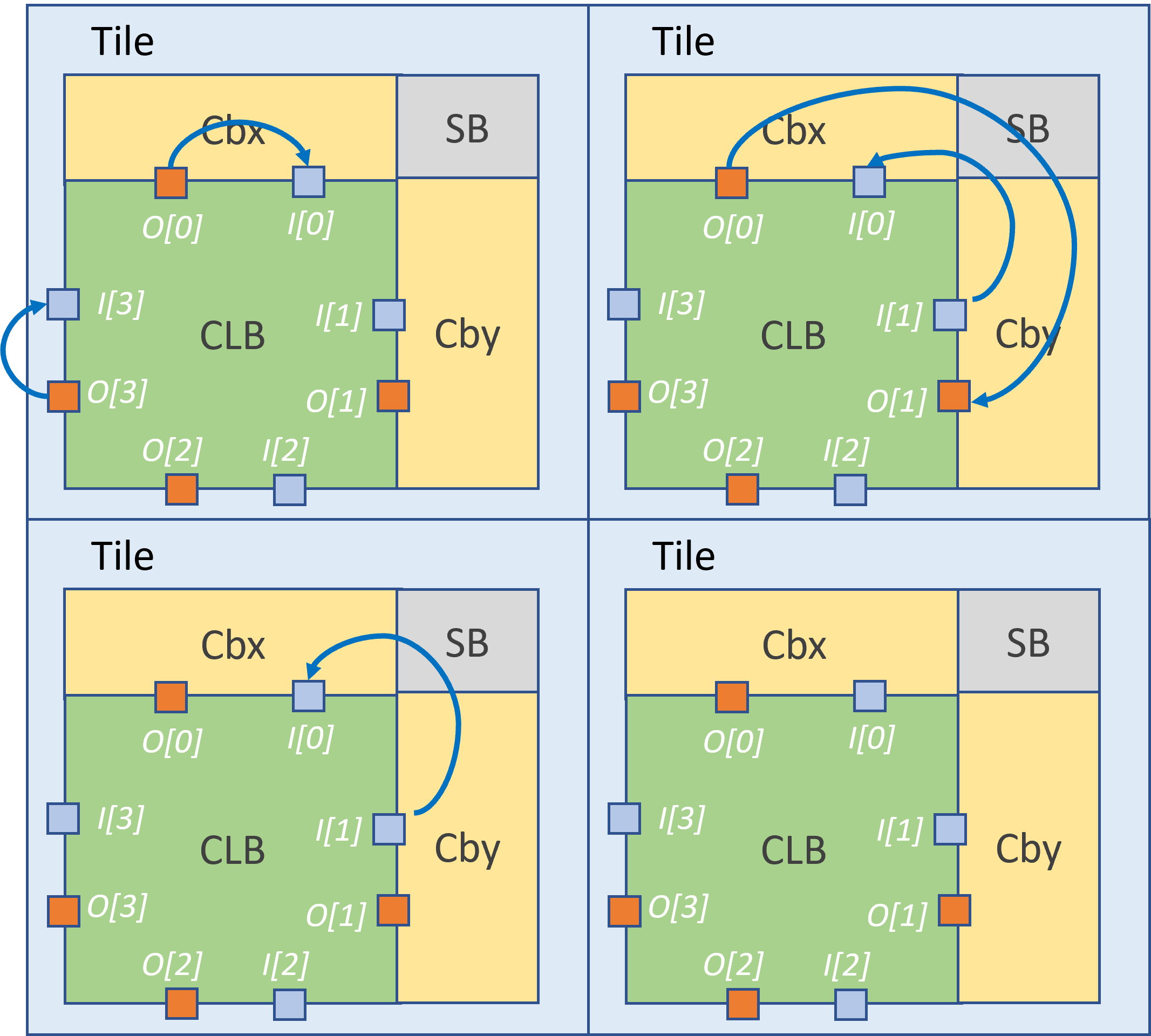
Fig. 49 Example of feedback connections inside a tile for enhanced connection block
For instance, a non-tileable VPR architecture defines:
<directlist>
  <!-- Add 2 inputs to the routing multiplexers inside a connection block which drives pin 'clb.I_top[0]' -->
  <direct name="feedback" from_pin="clb.O_top[0:0]" to_pin="clb.I_top[0:0]" x_offset="0" y_offset="0" z_offset="0"/>
  <direct name="feedback" from_pin="clb.O_top[1:1]" to_pin="clb.I_top[0:0]" x_offset="0" y_offset="0" z_offset="0"/>
</directlist>
Fig. 50 shows a few inter-tile connections which can be built inside connection blocks. Note that inter-tile connections are subjected to the restrictions depicted in Fig. 48
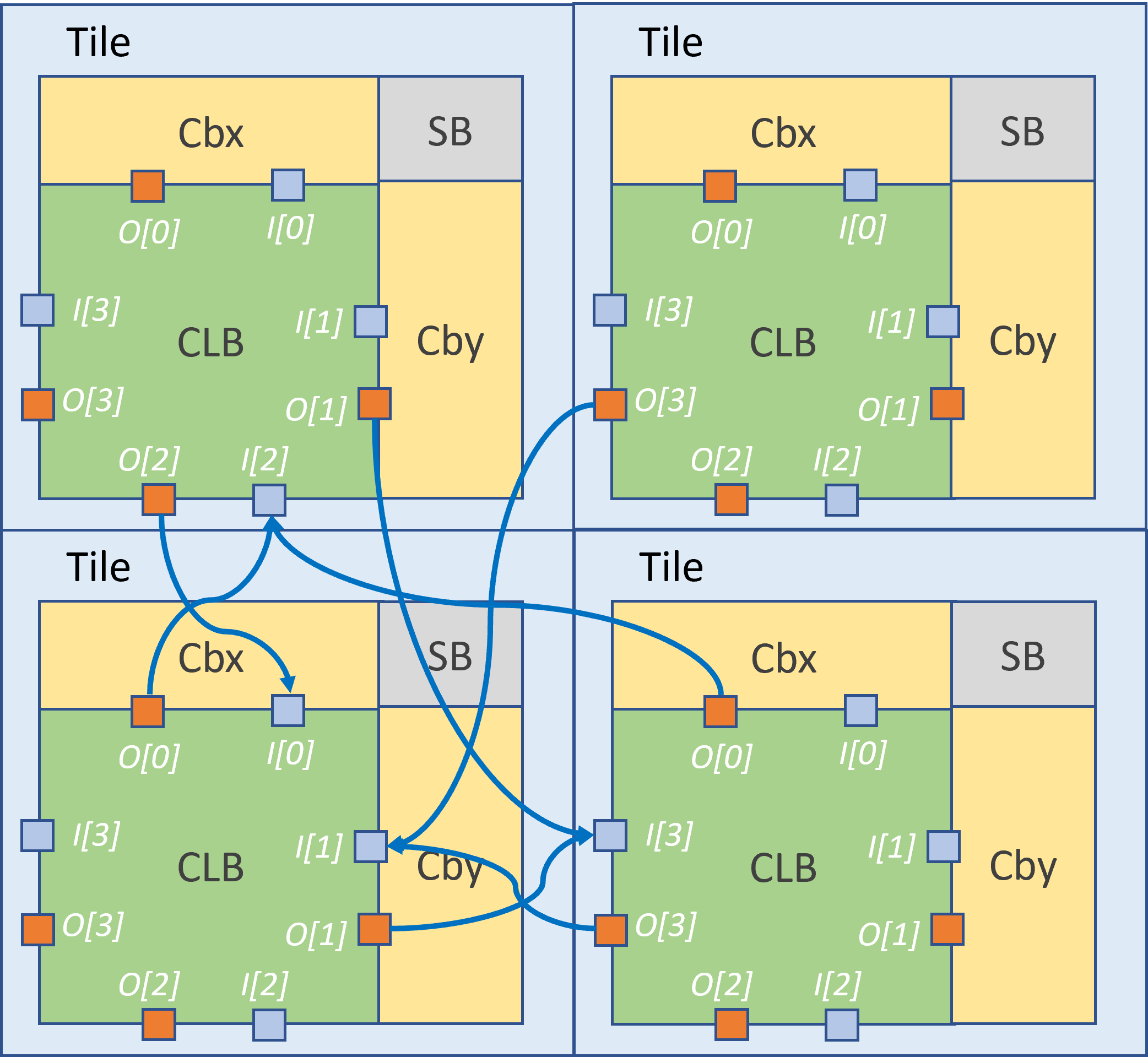
Fig. 50 Example of connections across two tiles for enhanced connection block
Fig. 51 illustrates some inner-tile and inter-tile connections which are not allowed. Note that feedback connections across different sides are restricted!
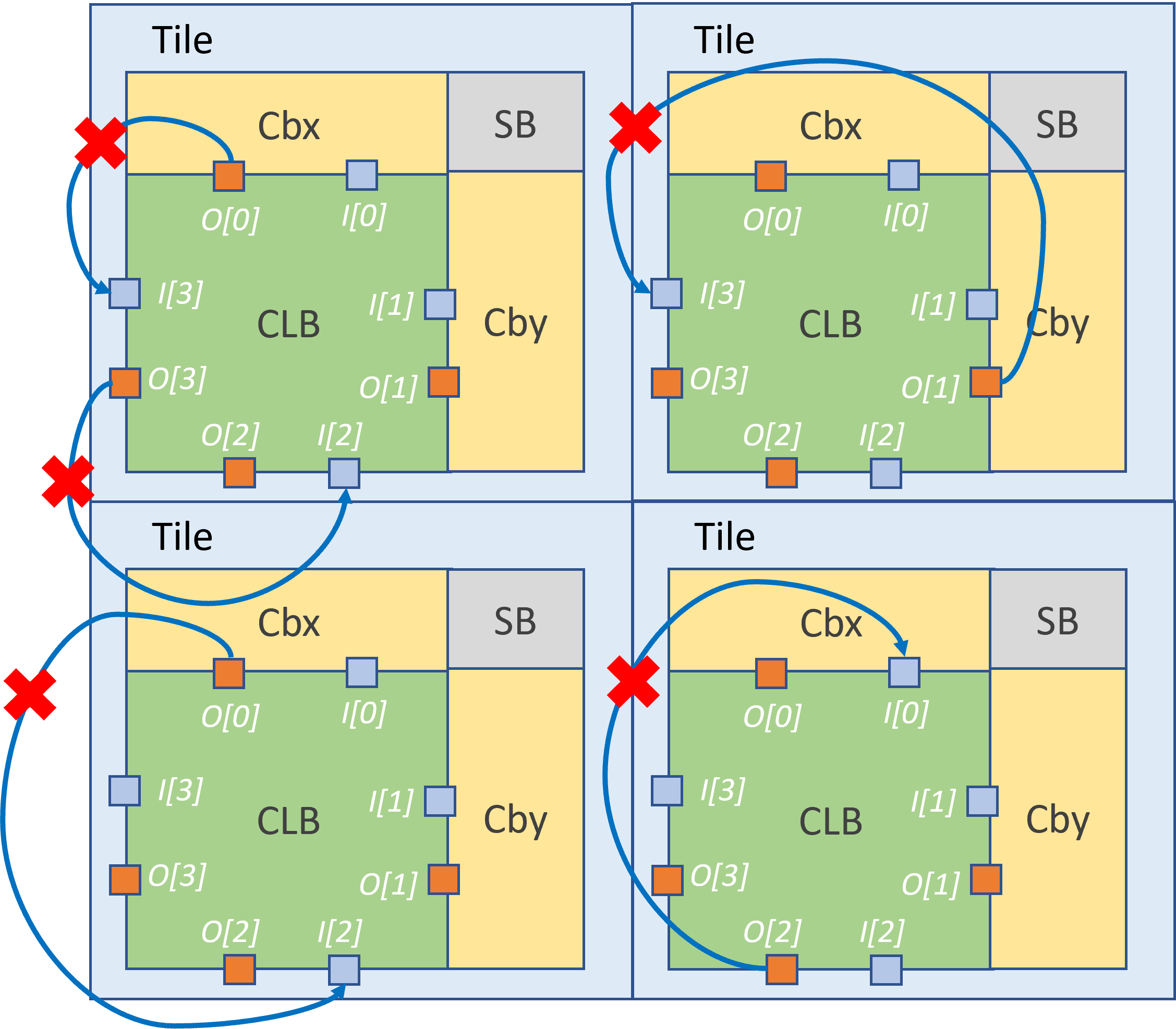
Fig. 51 Restrictions on building direct connections as part of a connection block
Inter-tile Connections
For this example, we will study a scan-chain implementation. The description could be:
In a non-tileable architecture:
<directlist>
  <direct name="scff_chain" from_pin="clb.sc_out" to_pin="clb.sc_in" x_offset="0" y_offset="-1" z_offset="0"/>
</directlist>
In a tileable architecture:
<direct_connection>
  <direct name="scff_chain" interconnection_type="column" x_dir="positive" y_dir="positive"/>
</direct_connection>
Fig. 52 is the graphical representation of the above scan-chain description on a 4x4 FPGA.
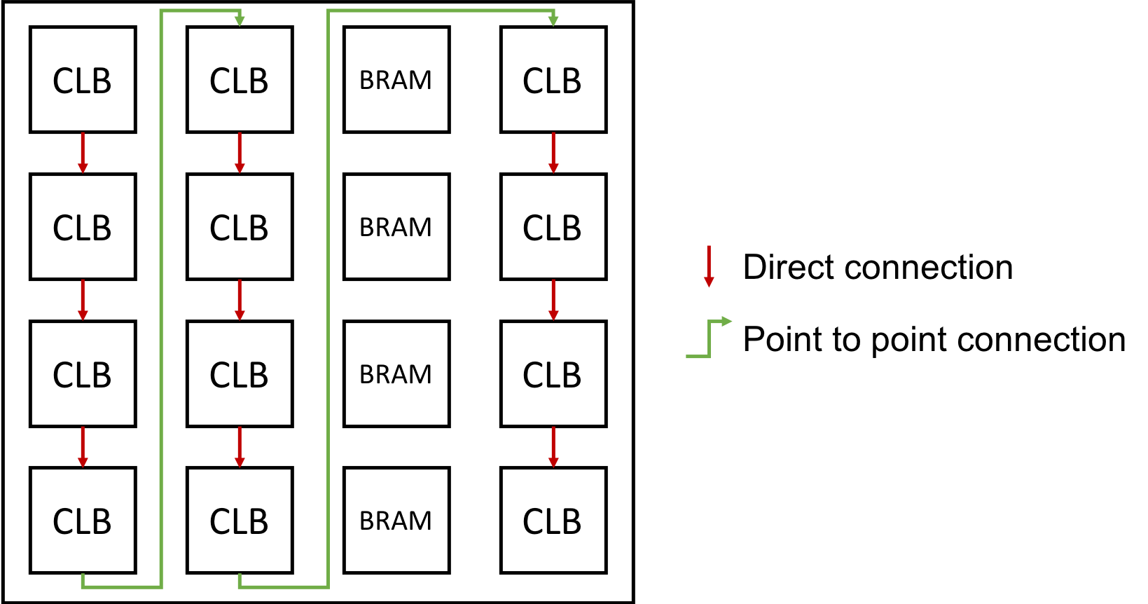
Fig. 52 An example of scan-chain implementation
In this figure, the red arrows represent the initial direct connection. The green arrows represent the point to point connection to connect all the columns of CLB.
A point to point connection can be applied in different ways than showed in the example section. To help the designer implement their point to point connection, a truth table with our new parameters is provided below.
Fig. 53 provides all possible variable combination and the connection it will generate.
Fig. 53 Point to point truth table