Post-Implementation Timing Simulation
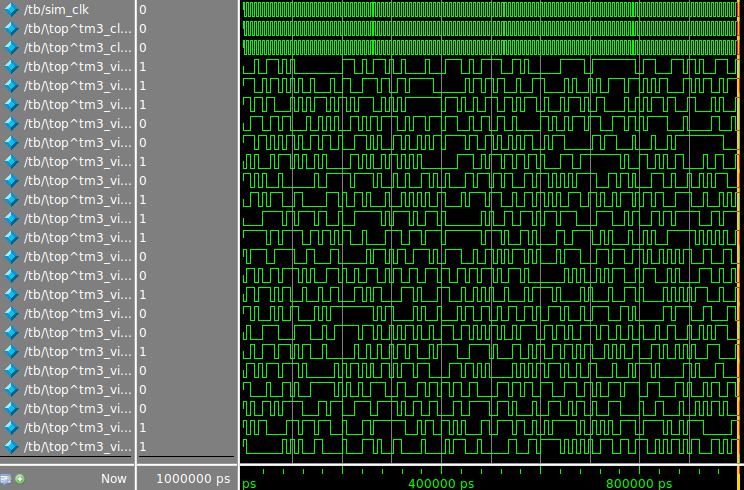
Fig. 95 Timing simulation waveform for stereovision3
This tutorial describes how to simulate a circuit which has been implemented by VPR with back-annotated timing delays.
- Back-annotated timing simulation is useful for a variety of reasons:
Checking that the circuit logic is correctly implemented
Checking that the circuit behaves correctly at speed with realistic delays
Generating VCD (Value Change Dump) files with realistic delays (e.g. for power estimation)
Generating the Post-Implementation Netlist
For the purposes of this tutorial we will be using the stereovision3 benchmark, and will target the k6_N10_40nm architecture.
First lets create a directory to work in:
$ mkdir timing_sim_tut
$ cd timing_sim_tut
Next we’ll copy over the stereovision3 benchmark netlist in BLIF format and the FPGA architecture description:
$ cp $VTR_ROOT/vtr_flow/benchmarks/vtr_benchmarks_blif/stereovision3.blif .
$ cp $VTR_ROOT/vtr_flow/arch/timing/k6_N10_40nm.xml .
Note
Replace $VTR_ROOT with the root directory of the VTR source tree
Now we can run VPR to implement the circuit onto the k6_N10_40nm architecture.
We also need to provide the vpr --gen_post_synthesis_netlist option to generate the post-implementation netlist and dump the timing information in Standard Delay Format (SDF):
$ vpr k6_N10_40nm.xml stereovision3.blif --gen_post_synthesis_netlist on
Once VPR has completed we should see the generated verilog netlist and SDF:
$ ls *.v *.sdf
sv_chip3_hierarchy_no_mem_post_synthesis.sdf  sv_chip3_hierarchy_no_mem_post_synthesis.v
Inspecting the Post-Implementation Netlist
Lets take a quick look at the generated files.
First is a snippet of the verilog netlist:
fpga_interconnect \routing_segment_lut_n616_output_0_0_to_lut_n497_input_0_4  (
    .datain(\lut_n616_output_0_0 ),
    .dataout(\lut_n497_input_0_4 )
);


//Cell instances
LUT_K #(
    .K(6),
    .LUT_MASK(64'b0000000000000000000000000000000000100001001000100000000100000010)
) \lut_n452  (
    .in({
        1'b0,
        \lut_n452_input_0_4 ,
        \lut_n452_input_0_3 ,
        \lut_n452_input_0_2 ,
        1'b0,
        \lut_n452_input_0_0 }),
    .out(\lut_n452_output_0_0 )
);

DFF #(
    .INITIAL_VALUE(1'b0)
) \latch_top^FF_NODE~387  (
    .D(\latch_top^FF_NODE~387_input_0_0 ),
    .Q(\latch_top^FF_NODE~387_output_0_0 ),
    .clock(\latch_top^FF_NODE~387_clock_0_0 )
);
Here we see three primitives instantiated:
fpga_interconnectrepresents connections between netlist primitivesLUT_Krepresents look-up tables (LUTs) (corresponding to.namesin the BLIF netlist). Two parameters define the LUTs functionality:Kthe number of inputs, andLUT_MASKwhich defines the logic function.
DFFrepresents a D-Flip-Flop (corresponding to.latchin the BLIF netlist).The
INITIAL_VALUEparameter defines the Flip-Flop’s initial state.
Different circuits may produce other types of netlist primitives corresponding to hardened primitive blocks in the FPGA such as adders, multipliers and single or dual port RAM blocks.
Note
The different primitives produced by VPR are defined in $VTR_ROOT/vtr_flow/primitives.v
Lets now take a look at the Standard Delay Format (SDF) file:
 1(CELL
 2    (CELLTYPE "fpga_interconnect")
 3    (INSTANCE routing_segment_lut_n616_output_0_0_to_lut_n497_input_0_4)
 4    (DELAY
 5        (ABSOLUTE
 6            (IOPATH datain dataout (312.648:312.648:312.648) (312.648:312.648:312.648))
 7        )
 8    )
 9)
10
11(CELL
12    (CELLTYPE "LUT_K")
13    (INSTANCE lut_n452)
14    (DELAY
15        (ABSOLUTE
16            (IOPATH in[0] out (261:261:261) (261:261:261))
17            (IOPATH in[2] out (261:261:261) (261:261:261))
18            (IOPATH in[3] out (261:261:261) (261:261:261))
19            (IOPATH in[4] out (261:261:261) (261:261:261))
20        )
21    )
22)
23
24(CELL
25    (CELLTYPE "DFF")
26    (INSTANCE latch_top\^FF_NODE\~387)
27    (DELAY
28        (ABSOLUTE
29            (IOPATH (posedge clock) Q (124:124:124) (124:124:124))
30        )
31    )
32    (TIMINGCHECK
33        (SETUP D (posedge clock) (66:66:66))
34    )
35)
The SDF defines all the delays in the circuit using the delays calculated by VPR’s STA engine from the architecture file we provided.
Here we see the timing description of the cells in Listing 28.
In this case the routing segment routing_segment_lut_n616_output_0_0_to_lut_n497_input_0_4 has a delay of 312.648 ps, while the LUT lut_n452 has a delay of 261 ps from each input to the output.
The DFF latch_top\^FF_NODE\~387 has a clock-to-q delay of 124 ps and a setup time of 66ps.
Creating a Test Bench
In order to simulate a benchmark we need a test bench which will stimulate our circuit (the Device-Under-Test or DUT).
An example test bench which will randomly perturb the inputs is shown below:
  1`timescale 1ps/1ps
  2module tb();
  3
  4localparam CLOCK_PERIOD = 8000;
  5localparam CLOCK_DELAY = CLOCK_PERIOD / 2;
  6
  7//Simulation clock
  8logic sim_clk;
  9
 10//DUT inputs
 11logic \top^tm3_clk_v0 ;
 12logic \top^tm3_clk_v2 ;
 13logic \top^tm3_vidin_llc ;
 14logic \top^tm3_vidin_vs ;
 15logic \top^tm3_vidin_href ;
 16logic \top^tm3_vidin_cref ;
 17logic \top^tm3_vidin_rts0 ;
 18logic \top^tm3_vidin_vpo~0 ;
 19logic \top^tm3_vidin_vpo~1 ;
 20logic \top^tm3_vidin_vpo~2 ;
 21logic \top^tm3_vidin_vpo~3 ;
 22logic \top^tm3_vidin_vpo~4 ;
 23logic \top^tm3_vidin_vpo~5 ;
 24logic \top^tm3_vidin_vpo~6 ;
 25logic \top^tm3_vidin_vpo~7 ;
 26logic \top^tm3_vidin_vpo~8 ;
 27logic \top^tm3_vidin_vpo~9 ;
 28logic \top^tm3_vidin_vpo~10 ;
 29logic \top^tm3_vidin_vpo~11 ;
 30logic \top^tm3_vidin_vpo~12 ;
 31logic \top^tm3_vidin_vpo~13 ;
 32logic \top^tm3_vidin_vpo~14 ;
 33logic \top^tm3_vidin_vpo~15 ;
 34
 35//DUT outputs
 36logic \top^tm3_vidin_sda ;
 37logic \top^tm3_vidin_scl ;
 38logic \top^vidin_new_data ;
 39logic \top^vidin_rgb_reg~0 ;
 40logic \top^vidin_rgb_reg~1 ;
 41logic \top^vidin_rgb_reg~2 ;
 42logic \top^vidin_rgb_reg~3 ;
 43logic \top^vidin_rgb_reg~4 ;
 44logic \top^vidin_rgb_reg~5 ;
 45logic \top^vidin_rgb_reg~6 ;
 46logic \top^vidin_rgb_reg~7 ;
 47logic \top^vidin_addr_reg~0 ;
 48logic \top^vidin_addr_reg~1 ;
 49logic \top^vidin_addr_reg~2 ;
 50logic \top^vidin_addr_reg~3 ;
 51logic \top^vidin_addr_reg~4 ;
 52logic \top^vidin_addr_reg~5 ;
 53logic \top^vidin_addr_reg~6 ;
 54logic \top^vidin_addr_reg~7 ;
 55logic \top^vidin_addr_reg~8 ;
 56logic \top^vidin_addr_reg~9 ;
 57logic \top^vidin_addr_reg~10 ;
 58logic \top^vidin_addr_reg~11 ;
 59logic \top^vidin_addr_reg~12 ;
 60logic \top^vidin_addr_reg~13 ;
 61logic \top^vidin_addr_reg~14 ;
 62logic \top^vidin_addr_reg~15 ;
 63logic \top^vidin_addr_reg~16 ;
 64logic \top^vidin_addr_reg~17 ;
 65logic \top^vidin_addr_reg~18 ;
 66
 67
 68//Instantiate the dut
 69sv_chip3_hierarchy_no_mem dut ( .* );
 70
 71//Load the SDF
 72initial $sdf_annotate("sv_chip3_hierarchy_no_mem_post_synthesis.sdf", dut);
 73
 74//The simulation clock
 75initial sim_clk = '1;
 76always #CLOCK_DELAY sim_clk = ~sim_clk;
 77
 78//The circuit clocks
 79assign \top^tm3_clk_v0 = sim_clk;
 80assign \top^tm3_clk_v2 = sim_clk;
 81
 82//Randomized input
 83always@(posedge sim_clk) begin
 84    \top^tm3_vidin_llc <= $urandom_range(1,0);
 85    \top^tm3_vidin_vs <= $urandom_range(1,0);
 86    \top^tm3_vidin_href <= $urandom_range(1,0);
 87    \top^tm3_vidin_cref <= $urandom_range(1,0);
 88    \top^tm3_vidin_rts0 <= $urandom_range(1,0);
 89    \top^tm3_vidin_vpo~0 <= $urandom_range(1,0);
 90    \top^tm3_vidin_vpo~1 <= $urandom_range(1,0);
 91    \top^tm3_vidin_vpo~2 <= $urandom_range(1,0);
 92    \top^tm3_vidin_vpo~3 <= $urandom_range(1,0);
 93    \top^tm3_vidin_vpo~4 <= $urandom_range(1,0);
 94    \top^tm3_vidin_vpo~5 <= $urandom_range(1,0);
 95    \top^tm3_vidin_vpo~6 <= $urandom_range(1,0);
 96    \top^tm3_vidin_vpo~7 <= $urandom_range(1,0);
 97    \top^tm3_vidin_vpo~8 <= $urandom_range(1,0);
 98    \top^tm3_vidin_vpo~9 <= $urandom_range(1,0);
 99    \top^tm3_vidin_vpo~10 <= $urandom_range(1,0);
100    \top^tm3_vidin_vpo~11 <= $urandom_range(1,0);
101    \top^tm3_vidin_vpo~12 <= $urandom_range(1,0);
102    \top^tm3_vidin_vpo~13 <= $urandom_range(1,0);
103    \top^tm3_vidin_vpo~14 <= $urandom_range(1,0);
104    \top^tm3_vidin_vpo~15 <= $urandom_range(1,0);
105end
106
107endmodule
The testbench instantiates our circuit as dut at line 69.
To load the SDF we use the $sdf_annotate() system task (line 72) passing the SDF filename and target instance.
The clock is defined on lines 75-76 and the random circuit inputs are generated at the rising edge of the clock on lines 84-104.
Performing Timing Simulation in Modelsim
To perform the timing simulation we will use Modelsim, an HDL simulator from Mentor Graphics.
Note
Other simulators may use different commands, but the general approach will be similar.
It is easiest to write a tb.do file to setup and configure the simulation:
 1#Enable command logging
 2transcript on
 3
 4#Setup working directories
 5if {[file exists gate_work]} {
 6    vdel -lib gate_work -all
 7}
 8vlib gate_work
 9vmap work gate_work
10
11#Load the verilog files
12vlog -sv -work work {sv_chip3_hierarchy_no_mem_post_synthesis.v}
13vlog -sv -work work {tb.sv}
14vlog -sv -work work {$VTR_ROOT/vtr_flow/primitives.v}
15
16#Setup the simulation
17vsim -t 1ps -L gate_work -L work -voptargs="+acc" +sdf_verbose +bitblast tb
18
19#Log signal changes to a VCD file
20vcd file sim.vcd
21vcd add /tb/dut/*
22vcd add /tb/dut/*
23
24#Setup the waveform viewer
25log -r /tb/*
26add wave /tb/*
27view structure
28view signals
29
30#Run the simulation for 1 microsecond
31run 1us -all
We link together the post-implementation netlist, test bench and VTR primitives on lines 12-14. The simulation is then configured on line 17, some of the options are worth discussing in more detail:
+bitblast: Ensures Modelsim interprets the primitives inprimitives.vcorrectly for SDF back-annotation.
Warning
Failing to provide +bitblast can cause errors during SDF back-annotation
+sdf_verbose: Produces more information about SDF back-annotation, useful for verifying that back-annotation succeeded.
Lastly, we tell the simulation to run on line 31.
Now that we have a .do file, lets launch the modelsim GUI:
$ vsim
and then run our .do file from the internal console:
ModelSim> do tb.do
Once the simulation completes we can view the results in the waveform view as shown in at the top of the page, or process the generated VCD file sim.vcd.