File Formats
VPR consumes and produces several files representing the packing, placement, and routing results.
FPGA Architecture (.xml)
The target FPGA architecture is specified as an architecture file. For details of this file format see FPGA Architecture Description.
BLIF Netlist (.blif)
The technology mapped circuit to be implement on the target FPGA is specified as a Berkely Logic Interchange Format (BLIF) netlist.
The netlist must be flattened and consist of only primitives (e.g. .names, .latch, .subckt).
For a detailed description of the BLIF file format see the BLIF Format Description.
Note that VPR supports only the structural subset of BLIF, and does not support the following BLIF features:
Subfile References (
.search).Finite State Machine Descriptions (
.start_kiss,.end_kissetc.).Clock Constraints (
.cycle,.clock_event).Delay Constraints (
.delayetc.).
Clock and delay constraints can be specified with an SDC File.
Note
By default VPR assumes file with .blif are in structural BLIF format. The format can be controlled with vpr --circuit_format.
Black Box Primitives
Black-box architectural primitives (RAMs, Multipliers etc.) should be instantiated in the netlist using BLIF’s .subckt directive.
The BLIF file should also contain a black-box .model definition which defines the input and outputs of each .subckt type.
VPR will check that blackbox .models are consistent with the <models> section of the architecture file.
Unconnected Primitive Pins
Unconnected primitive pins can be specified through several methods.
The
unconnnet (input pins only).VPR treats any input pin connected to a net named
unconnas disconnected.For example:
.names unconn out
0 1
specifies an inverter with no connected input.
Note
unconnshould only be used for input pins. It may cause name conflicts and create multi-driven nets if used with output pins.Implicitly disconnected
.subcktpins.For
.subcktinstantiations VPR treats unlisted primitive pins as implicitly disconnected. This works for both input and output pins.For example the following
.subcktinstantiations are equivalent:.subckt single_port_ram \ clk=top^clk \ data=top.memory_controller+memtroll^MULTI_PORT_MUX~8^MUX_2~546 \ addr[0]=top.memory_controller+memtroll^MULTI_PORT_MUX~8^MUX_2~541 \ addr[1]=top.memory_controller+memtroll^MULTI_PORT_MUX~8^MUX_2~542 \ addr[2]=top.memory_controller+memtroll^MULTI_PORT_MUX~8^MUX_2~543 \ addr[3]=top.memory_controller+memtroll^MULTI_PORT_MUX~8^MUX_2~544 \ addr[4]=top.memory_controller+memtroll^MULTI_PORT_MUX~8^MUX_2~545 \ addr[5]=unconn \ addr[6]=unconn \ addr[7]=unconn \ addr[8]=unconn \ addr[9]=unconn \ addr[10]=unconn \ addr[11]=unconn \ addr[12]=unconn \ addr[13]=unconn \ addr[14]=unconn \ we=top.memory_controller+memtroll^MULTI_PORT_MUX~8^MUX_2~554 \ out=top.memory_controller+memtroll.single_port_ram+str^out~0.subckt single_port_ram \ clk=top^clk \ data=top.memory_controller+memtroll^MULTI_PORT_MUX~8^MUX_2~546 \ addr[0]=top.memory_controller+memtroll^MULTI_PORT_MUX~8^MUX_2~541 \ addr[1]=top.memory_controller+memtroll^MULTI_PORT_MUX~8^MUX_2~542 \ addr[2]=top.memory_controller+memtroll^MULTI_PORT_MUX~8^MUX_2~543 \ addr[3]=top.memory_controller+memtroll^MULTI_PORT_MUX~8^MUX_2~544 \ addr[4]=top.memory_controller+memtroll^MULTI_PORT_MUX~8^MUX_2~545 \ we=top.memory_controller+memtroll^MULTI_PORT_MUX~8^MUX_2~554 \ out=top.memory_controller+memtroll.single_port_ram+str^out~0Dummy nets with no sinks (output pins only)
By default VPR sweeps away nets with no sinks (see
vpr --sweep_dangling_nets). As a result output pins can be left ‘disconnected’ by connecting them to dummy nets.For example:
.names in dummy_net1
0 1
specifies an inverter with no connected output (provided
dummy_net1is connected to no other pins).Note
This method requires that every disconnected output pin should be connected to a uniquely named dummy net.
BLIF File Format Example
The following is an example BLIF file. It implements a 4-bit ripple-carry adder and some simple logic.
The main .model is named top, and its input and output pins are listed using the .inputs and .outputs directives.
The 4-bit ripple-cary adder is built of 1-bit adder primitives which are instantiated using the .subckt directive.
Note that the adder primitive is defined as its own .model (which describes its pins), and is marked as .blackbox to indicate it is an architectural primitive.
The signal all_sum_high_comb is computed using combinational logic (.names) which ANDs all the sum bits together.
The .latch directive instantiates a rising-edge (re) latch (i.e. an edge-triggered Flip-Flop) clocked by clk.
It takes in the combinational signal all_sum_high_comb and drives the primary output all_sum_high_reg.
Also note that the last .subckt adder has it’s cout output left implicitly disconnected.
.model top
.inputs clk a[0] a[1] a[2] a[3] b[0] b[1] b[2] b[3]
.outputs sum[0] sum[1] sum[2] sum[3] cout all_sum_high_reg

.names gnd
 0

.subckt adder a=a[0] b=b[0] cin=gnd    cout=cin[1]     sumout=sum[0]
.subckt adder a=a[1] b=b[1] cin=cin[1] cout=cin[2]     sumout=sum[1]
.subckt adder a=a[2] b=b[2] cin=cin[2] cout=cin[3]     sumout=sum[2]
.subckt adder a=a[3] b=b[3] cin=cin[3]                 sumout=sum[3]

.names sum[0] sum[1] sum[2] sum[3] all_sum_high_comb
1111 1

.latch all_sum_high_comb all_sum_high_reg re clk  0

.end


.model adder
.inputs a b cin
.outputs cout sumout
.blackbox
.end
BLIF Naming Convention
VPR follows a naming convention to refer to primitives and pins in the BLIF netlist. These names appear in the VPR GUI, in log and error messages, and in can be used elsewhere (e.g. in SDC constraints).
Net Names
The BLIF format uses explicit names to refer to nets. These names are used directly as is by VPR (although some nets may be merged/removed by netlist cleaning).
For example, the following netlist:
.model top
.inputs a b
.outputs c

.names a b c
11 1

.end
contains nets named:
abc
Primitive Names
The standard BLIF format has no mechanism for specifying the names of primitives (e.g. .names/.latch/.subckt).
As a result, tools processing BLIF follow a naming convention which generates unique names for each netlist primitive.
The VPR primitive naming convention is as follows:
Primitive |
Drives at least one net? |
Primitive Name |
|---|---|---|
|
Yes |
Name of first driven net |
No |
Arbitrarily
generated (e.g.
|
|
|
N/A |
.output name
prefixed with
|
which ensures each netlist primitive is given a unique name.
For example, in the following:
.model top
.inputs a b x y z clk
.outputs c c_reg cout[0] sum[0]

.names a b c
11 1

.latch c c_reg re clk 0

.subckt adder a=x b=y cin=z cout=cout[0] sumout=sum[0]

.end

.model adder
.inputs a b cin
.outputs cout sumout
.blackbox
.end
The circuit primary inputs (
.inputs) are named:a,b,x,y,z,clk,The 2-LUT (
.names) is namedc,The FF (
.latch) is namedc_reg,The
adder(.subckt) is namedcout[0](the name of the first net it drives), andThe circuit primary outputs (
.outputs) are named:out:c,out:c_reg,out:cout[0],out:sum[0].
See also
EBLIF’s .cname extension, which allows explicit primitive names to be specified.
Pin Names
It is useful to be able to refer to particular pins in the netlist.
VPR uses the convention: <primitive_instance_name>.<pin_name>.
Where <primitive_instance_name> is replaced with the netlist primitive name, and <pin_name> is the name of the relevant pin.
For example, the following adder:
.subckt adder a=x b=y cin=z cout=cout[0] sumout=sum[0]
which has pin names:
cout[0].a[0](driven by netx)cout[0].b[0](driven by nety)cout[0].cin[0](driven by netz)cout[0].cout[0](drives netcout[0])cout[0].sumout[0](drives netsum[0])
Since the primitive instance itself is named cout[0] by convention.
Built-in Primitive Pin Names
The built-in primitives in BLIF (.names, .latch) do not explicitly list the names of their input/output pins.
VPR uses the following convention:
Primitive |
Port |
Name |
|---|---|---|
|
input |
|
output |
|
|
|
input |
|
output |
|
|
control |
|
Consider the following:
.names a b c d e f
11111 1

.latch g h re clk 0
The .names pin names are:
f.in[0](driven by neta)f.in[1](driven by netb)f.in[2](driven by netc)f.in[3](driven by netd)f.in[4](driven by nete)f.out[0](drives netf)
and the .latch pin names are:
h.D[0](driven by netg)h.Q[0](drives neth)h.clk[0](driven by netclk)
since the .names and .latch primitives are named f and h by convention.
Note
To support pins within multi-bit ports unambiguously, the bit index of the pin within its associated port is included in the pin name (for single-bit ports this will always be [0]).
Extended BLIF (.eblif)
VPR also supports several extensions to structural BLIF to address some of its limitations.
Note
By default VPR assumes file with .eblif are in extneded BLIF format. The format can be controlled with vpr --circuit_format.
.conn
The .conn statement allows direct connections between two wires.
For example:
.model top
.input a
.output b

#Direct connection
.conn a b

.end
specifies that ‘a’ and ‘b’ are direct connected together.
This is analogous to Verilog’s assign b = a;.
This avoids the insertion of a .names buffer which is required in standard BLIF, for example:
.model top
.input a
.output b

#Buffer LUT required in standard BLIF
.names a b
1 1

.end
.cname
The .cname statement allows names to be specified for BLIF primitives (e.g. .latch, .names, .subckt).
Note
.cname statements apply to the previous primitive instantiation.
For example:
.names a b c
11 1
.cname my_and_gate
Would name of the above .names instance my_and_gate.
.param
The .param statement allows parameters (e.g. primitive modes) to be tagged on BLIF primitives.
Note
.param statements apply to the previous primitive instantiation.
Parameters can have one of the three available types. Type is inferred from the format in which a parameter is provided.
- string
Whenever a parameter value is quoted it is considered to be a string. BLIF parser does not allow escaped characters hence those are illegal and will cause syntax errors.
- binary word
Binary words are specified using strings of characters
0and1. No other characters are allowed. Number of characters denotes the word length.
- real number
Real numbers are stored as decimals where the dot
.character separates the integer and fractional part. Presence of the dot character implies that the value is to be treated as a real number.
For example:
.subckt pll clk_in=gclk clk_out=pclk
.param feedback "internal"
.param multiplier 0.50
.param power 001101
Would set the parameters feedback, multiplier and power of the above pll .subckt to "internal", 0.50 and 001101 respectively.
Warning
Integers in notation other than binary (e.g. decimal, hexadecimal) are not supported. Occurrence of params with digits other than 1 and 0 for binary words, not quoted (strings) or not separated with dot . (real numbers) are considered to be illegal.
Interpretation of parameter values is out of scope of the BLIF format extension.
.param statements propagate to <parameter> elements in the packed netlist.
Paramerer values propagate also to the post-route Verilog netlist, if it is generated. Strings and real numbers are passed directly while binary words are prepended with the <N>'b prefix where N denotes a binary word length.
.attr
The .attr statement allows attributes (e.g. source file/line) to be tagged on BLIF primitives.
Note
.attr statements apply to the previous primitive instantiation.
For example:
.latch a_and_b dff_q re clk 0
.attr src my_design.v:42
Would set the attribute src of the above .latch to my_design.v:42.
.attr statements propagate to <attribute> elements in the packed netlist.
Extended BLIF File Format Example
.model top
.inputs a b clk
.outputs o_dff

.names a b a_and_b
11 1
.cname lut_a_and_b
.param test_names_param "test_names_param_value"
.attr test_names_attrib "test_names_param_attrib"

.latch a_and_b dff_q re clk 0
.cname my_dff
.param test_latch_param "test_latch_param_value"
.attr test_latch_attrib "test_latch_param_attrib"

.conn dff_q o_dff

.end
Timing Constraints (.sdc)
Timing constraints are specified using SDC syntax. For a description of VPR’s SDC support see SDC Commands.
Note
Use vpr --sdc_file to specify the SDC file used by VPR.
Timing Constraints File Format Example
See SDC Examples.
Packed Netlist Format (.net)
The circuit .net file is an xml file that describes a post-packed user circuit. It represents the user netlist in terms of the complex logic blocks of the target architecture. This file is generated from the packing stage and used as input to the placement stage in VPR.
The .net file is constructed hierarchically using block tags.
The top level block tag contains the I/Os and complex logic blocks used in the user circuit.
Each child block tag of this top level tag represents a single complex logic block inside the FPGA.
The block tags within a complex logic block tag describes, hierarchically, the clusters/modes/primitives used internally within that logic block.
A block tag has the following attributes:
nameA name to identify this component of the FPGA. This name can be completely arbitrary except in two situations. First, if this is a primitive (leaf) block that implements an atom in the input technology-mapped netlist (eg. LUT, FF, memory slice, etc), then the name of this block must match exactly with the name of the atom in that netlist so that one can later identify that mapping. Second, if this block is not used, then it should be named with the keyword open. In all other situations, the name is arbitrary.
instanceThe physical block in the FPGA architecture that the current block represents. Should be of format: architecture_instance_name[instance #]. For example, the 5th index BLE in a CLB should have
instance="ble[5]"
modeThe mode the block is operating in.
A block connects to other blocks via pins which are organized based on a hierarchy. All block tags contains the children tags: inputs, outputs, clocks. Each of these tags in turn contain port tags. Each port tag has an attribute name that matches with the name of a corresponding port in the FPGA architecture. Within each port tag is a list of named connections where the first name corresponds to pin 0, the next to pin 1, and so forth. The names of these connections use the following format:
Unused pins are identified with the keyword open.
The name of an input pin to a complex logic block is the same as the name of the net using that pin.
The name of an output pin of a primitive (leaf block) is the same as the name of the net using that pin.
The names of all other pins are specified by describing their immediate drivers. This format is
[name_of_immediate_driver_block].[port_name][pin#]->interconnect_name.
For primitives with equivalent inputs VPR may rotate the input pins.
The resulting rotation is specified with the <port_rotation_map> tag.
For example, consider a netlist contains a 2-input LUT named c, which is implemented in a 5-LUT:
 1...
 2<block name="c" instance="lut[0]">
 3    <inputs>
 4        <port name="in">open open lut5.in[2]->direct:lut5  open lut5.in[4]->direct:lut5  </port>
 5        <port_rotation_map name="in">open open 1 open 0 </port_rotation_map>
 6    </inputs>
 7    <outputs>
 8        <port name="out">c </port>
 9    </outputs>
10    <clocks>
11    </clocks>
12</block>
13...
In the original netlist the two LUT inputs were connected to pins at indices 0 and 1 (the only input pins).
However during clustering the inputs were rotated, and those nets now connect to the pins at indices 2 and 4 (line 4).
The <port_rotation_map> tag specified the port name it applies to (name attribute), and its contents lists the pin indices each pin in the port list is associated with in the original netlist (i.e. the pins lut5.in[2]->direct:lut5 and lut5.in[4]->direct:lut5 respectively correspond to indices 1 and 0 in the original netlist).
Note
Use vpr --net_file to override the default net file name.
Packing File Format Example
The following is an example of what a .net file would look like. In this circuit there are 3 inputs (pa, pb, pc) and 4 outputs (out:pd, out:pe, out:pf, out:pg). The io pad is set to inpad mode and is driven by the inpad:
 1<block name="b1.net" instance="FPGA_packed_netlist[0]">
 2    <inputs>
 3            pa pb pc
 4    </inputs>
 5
 6    <outputs>
 7            out:pd out:pe out:pf out:pg
 8    </outputs>
 9
10    <clocks>
11    </clocks>
12
13    <block name="pa" instance="io[0]" mode="inpad">
14            <inputs>
15                    <port name="outpad">open </port>
16            </inputs>
17
18            <outputs>
19                    <port name="inpad">inpad[0].inpad[0]->inpad  </port>
20            </outputs>
21
22            <clocks>
23                    <port name="clock">open </port>
24            </clocks>
25
26            <block name="pa" instance="inpad[0]">
27                    <inputs>
28                    </inputs>
29
30                    <outputs>
31                            <port name="inpad">pa </port>
32                    </outputs>
33
34                    <clocks>
35                    </clocks>
36
37                    <attributes>
38                            <attribute name="vccio">3.3</attribute>
39                    </attributes>
40
41                    <parameters>
42                            <parameter name="iostandard">LVCMOS33</parameter>
43                    </parameters>
44            </block>
45    </block>
46...
Note
.net files may be outputted at two stages:
- After packing is completed, the packing results will be outputted. The .net file can be loaded as an input for placer, router and analyzer. Note that the file may not represent the final packing results as the analyzer will apply synchronization between packing and routing results.
- After analysis is completed, updated packing results will be outputted. This is due to that VPR router may swap pin mapping in packing results for optimizations. In such cases, packing results are synchronized with routing results. The outputted .net file will have a postfix of .post_routing as compared to the original packing results. It could happen that VPR router does not apply any pin swapping and the two .net files are the same. In both cases, the post-analysis .net file should be considered to be the final packing results for downstream tools, e.g., bitstream generator. Users may load the post-routing .net file in VPR’s analysis flow to sign-off the final results.
Warning
Currently, the packing result synchronization is only applicable to input pins which may be remapped to different nets during routing optimization. If your architecture defines link_instance_pin_xml_syntax_ equivalence for output pins, the packing results still mismatch the routing results!
Placement File Format (.place)
The placement file format is used to specify the position of cluster-level blocks in an FPGA design. It includes information about the netlist and architecture files, the size of the logic block array, and the placement details of each block in the CLB netlist..
The first line of the placement file lists the netlist (.net) and architecture (.xml) files used to create this placement. This information is used to ensure you are warned if you accidentally route this placement with a different architecture or netlist file later. The second line of the file gives the size of the logic block array used by this placement.
All subsequent lines follow this format:
block_name x y subblk [layer_number] [#block_number]
block_name: Refers to either: - The name of a clustered block, as given in the input .net formatted netlist. - The name of a primitive within a clustered block.
x and y: Represent the row and column in which the block is placed, respectively.
subblk: Specifies which of several possible subtile locations in row x and column y contains this block, which is useful when the tile capacity is greater than 1. The subtile number should be in the range 0 to (grid[i][j].capacity - 1). The subtile numbers for a particular x, y location do not have to be used in order.
layer_number: Indicates the layer (or die) on which the block is placed. If omitted, the block is assumed to be placed on layer 0 (a single die system). In 3D FPGA architectures, multiple dies can be stacked, with the bottom die considered as layer 0.
The placement files output by VPR also include (as a comment) an extra field: the id (number) of the block in the CLB netlist. This is the internal index used by VPR to identify a CLB level block – it may be useful to know this index if you are modifying VPR and trying to debug something.
Note
The blocks in a placement file can be listed in any order.
Note
A # character on a line indicates that all text after the # to the end of a line is a comment.
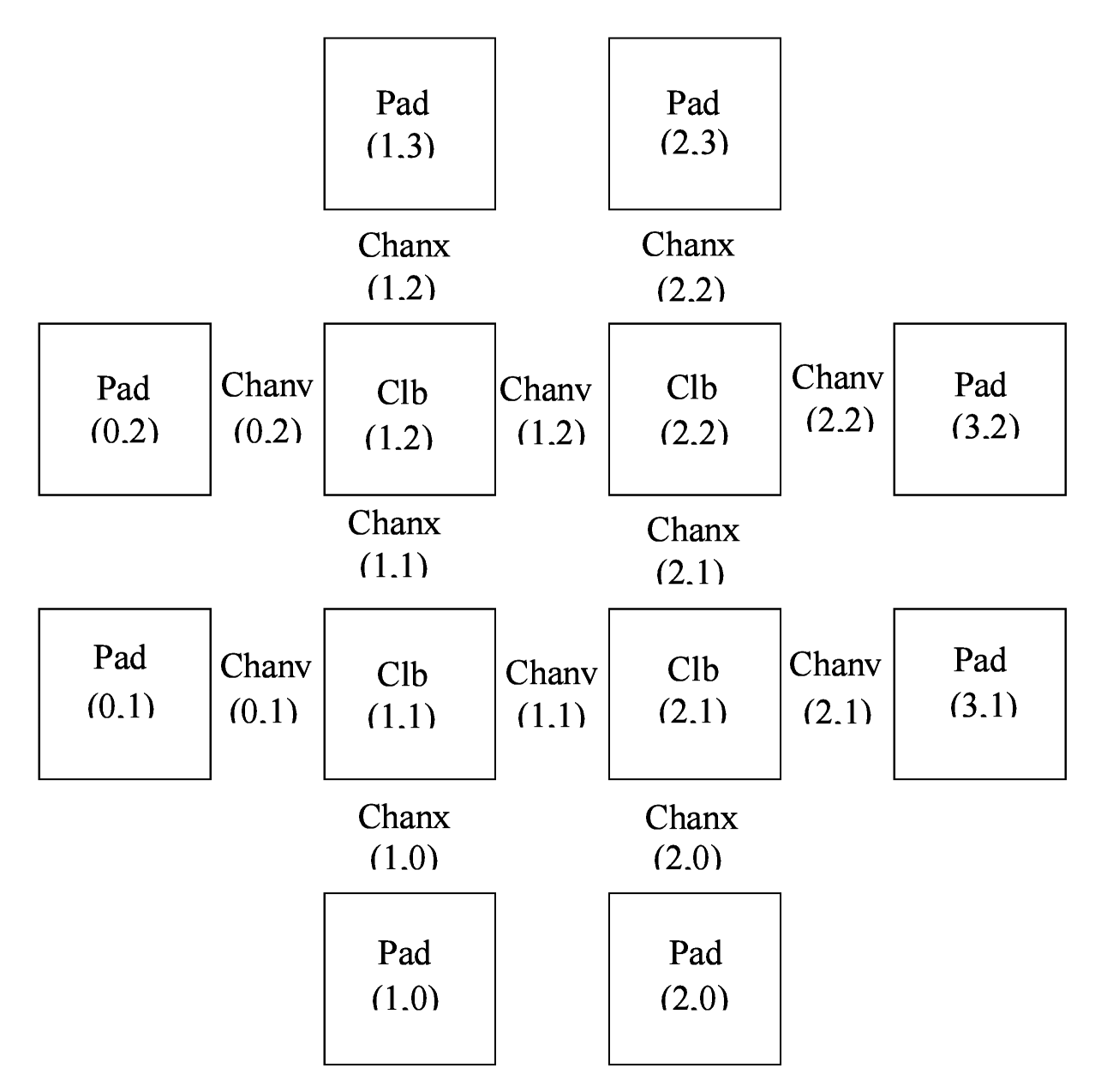
Fig. 71 FPGA coordinate system.
Fig. 71 shows the coordinate system used by VPR for a small 2 x 2 CLB FPGA.
The number of CLBs in the x and y directions are denoted by nx and ny, respectively.
CLBs all go in the area with x between 1 and nx and y between 1 and ny, inclusive.
All pads either have x equal to 0 or nx + 1 or y equal to 0 or ny + 1.
Note
Use vpr --place_file to override the default place file name.
Placement File Format Example
 1Netlist file: xor5.net   Architecture file: sample.xml
 2Array size: 2 x 2 logic blocks
 3
 4#block name x       y       subblk  block number
 5#---------- --      --      ------- -----------
 6a           0       1       0       #0  -- NB: block number is a comment.
 7b           1       0       0       #1
 8c           0       2       1       #2
 9d           1       3       0       #3
10e           1       3       1       #4
11out:xor5    0       2       0       #5
12xor5        1       2       0       #6
13[1]         1       1       0       #7
 1Netlist file: xor5.net   Architecture file: sample.xml
 2Array size: 2 x 2 logic blocks
 3
 4#block name x       y       subblk  layer  block number
 5#---------- --      --      ------- ------ -----------
 6a           0       1       0       0      #0  -- NB: block number is a comment.
 7b           1       0       0       1      #1
 8c           0       2       1       0      #2
 9d           1       3       0       1      #3
10e           1       3       1       0      #4
11out:xor5    0       2       0       1      #5
12xor5        1       2       0       0      #6
13[1]         1       1       0       1      #7
Flat Placement File Format (.fplace)
The flat placement file is a text file where each line describes the location of an atom. Each line in the flat placement file should have the following syntax:
<atom_name : str> <x : float> <y : float> <layer : float> <atom_sub_tile : int>
For example:
n523  6 8 0 0
n522  6 8 0 0
n520  6 9 0 0
n518  6 9 0 0
The position of the atom on the FPGA is given by 3 floating point values
(x, y, layer). We allow x and y locations to be off-grid since
this flat placement will be fed into the packer and placer, which will snap
the positions to grid locations. For 2D FPGA architectures, the layer should be 0.
The sub_tile is a clustered placement construct: which cluster-level
location at a given (x, y, layer) should these atoms go at (relevant when
multiple clusters can be stacked there). A sub-tile of -1 may be used when
the sub-tile of an atom is unknown (allowing the packing algorithm to choose
any sub-tile at the given (x, y, layer) location).
When used with flat-recon full legalizer (see vpr --ap_full_legalizer),
each atom in a molecule should have compatible location information. It is legal to
leave some molecules unconstrained; the reconstruction phase will choose where
to place them but does not attempt to optimize these locations.
Routing File Format (.route)
The first line of the routing file gives the array size, nx x ny.
The remainder of the routing file lists the global or the detailed routing for each net, one by one.
Each routing begins with the word net, followed by the net index used internally by VPR to identify the net and, in brackets, the name of the net given in the netlist file.
The following lines define the routing of the net.
Each begins with a keyword that identifies a type of routing segment.
The possible keywords are SOURCE (the source of a certain output pin class), SINK (the sink of a certain input pin class), OPIN (output pin), IPIN (input pin), CHANX (horizontal channel), and CHANY (vertical channel).
Each routing begins on a SOURCE and ends on a SINK.
In brackets after the keyword is the (x, y) location of this routing resource.
Finally, the pad number (if the SOURCE, SINK, IPIN or OPIN was on an I/O pad), pin number (if the IPIN or OPIN was on a clb), class number (if the SOURCE or SINK was on a clb) or track number (for CHANX or CHANY) is listed – whichever one is appropriate.
The meaning of these numbers should be fairly obvious in each case.
If we are attaching to a pad, the pad number given for a resource is the subblock number defining to which pad at location (x, y) we are attached.
See Fig. 71 for a diagram of the coordinate system used by VPR.
In a horizontal channel (CHANX) track 0 is the bottommost track, while in a vertical channel (CHANY) track 0 is the leftmost track.
Note that if only global routing was performed the track number for each of the CHANX and CHANY resources listed in the routing will be 0, as global routing does not assign tracks to the various nets.
For an N-pin net, we need N-1 distinct wiring “paths” to connect all the pins.
The first wiring path will always go from a SOURCE to a SINK.
The routing segment listed immediately after the SINK is the part of the existing routing to which the new path attaches.
Note
It is important to realize that the first pin after a SINK is the connection into the already specified routing tree; when computing routing statistics be sure that you do not count the same segment several times by ignoring this fact.
Note
Use vpr --route_file to override the default route file name.
Routing File Format Examples
An example routing for one net is listed below:
 1Net 5 (xor5)
 2
 3Node:  1   SOURCE (1,2)  Class: 1  Switch: 1       # Source for pins of class 1.
 4Node:  2   OPIN (1,2)    Pin: 4    clb.O[12]  Switch:0   #Output pin the O port of clb block, pin number 12
 5Node:  4   CHANX (1,1) to (4,1)  Track: 1  Switch: 1
 6Node:  6   CHANX (4,1) to (7,1)  Track: 1  Switch: 1
 7Node:  8   IPIN (7,1)  Pin: 0  clb.I[0]  Switch: 2
 8Node:  9   SINK (7,1)  Class: 0  Switch: -1      # Sink for pins of class 0 on a clb.
 9Node:  4   CHANX (7,1) to (10,1)  Track: 1  Switch: 1      # Note:  Connection to existing routing!
10Node:  5   CHANY (10,1) to (10,4)  Track: 1  Switch: 0
11Node:  4   CHANX (10,4) to (13,4)  Track: 1  Switch: 1
12Node:  10  CHANX (13,4) to (16,4)  Track: 1  Switch: 1
13Node:  11  IPIN (16,4)  Pad: 1  clb.I[1]  Switch: 2
14Node:  12  SINK (16,4)  Pad: 1  Switch: -1      # This sink is an output pad at (16,4), subblock 1.
Nets which are specified to be global in the netlist file (generally clocks) are not routed. Instead, a list of the blocks (name and internal index) which this net must connect is printed out. The location of each block and the class of the pin to which the net must connect at each block is also printed. For clbs, the class is simply whatever class was specified for that pin in the architecture input file. For pads the pinclass is always -1; since pads do not have logically-equivalent pins, pin classes are not needed. An example listing for a global net is given below.
1Net 146 (pclk): global net connecting:
2Block pclk (#146) at (1,0), pinclass -1
3Block pksi_17_ (#431) at (3,26), pinclass 2
4Block pksi_185_ (#432) at (5,48), pinclass 2
5Block n_n2879 (#433) at (49,23), pinclass 2
Routing Resource Graph File Format (.xml)
The routing resource graph (rr graph) file is an XML file that describes the routing resources within the FPGA.
VPR can generate a rr graph that matches your architecture specifications (from the architecture xml file), or it can read in an externally generated rr graph.
When this file is written by VPR, the rr graph written out is the rr graph generated before routing with a final channel width
(even if multiple routings at different channel widths are performed during a binary search for the minimum channel width).
When reading in rr graph from an external file, the rr graph is used during both the placement and routing phases of VPR.
The file is constructed using tags. The top level is the rr_graph tag.
This tag contains all the channel, switches, segments, block, grid, node, and edge information of the FPGA.
It is important to keep all the values as high precision as possible. Sensitive values include capacitance and Tdel. As default, these values are printed out with a precision of 30 digits.
Each of these sections are separated into separate tags as described below.
Note
Use vpr --read_rr_graph to specify an RR graph file to be loaded.
Note
Use vpr --write_rr_graph to specify where the RR graph should be written.
Detailed Tag Information
Channel
The channel information is contained within the channels subtag. This describes the minimum and maximum channel width within the architecture. Each channels tag has the following subtags:
- <channel chan_width_max="int" x_min="int" y_min="int" x_max="int" y_max="int"/>" title="Link to this definition">
This is a required subtag that contains information about the general channel width information. This stores the channel width between x or y directed channels.
- Required Attributes:
chan_width_max – Stores the maximum channel width value of x or y channels.
x_min y_min x_max y_max – Stores the minimum and maximum value of x and y coordinate within the lists.
-
<x_list index="int" info="int"/> <y_list index="int" info="int"/>
These are a required subtags that lists the contents of an x_list and y_list array which stores the width of each channel. The x_list array size as large as the size of the y dimension of the FPGA itself while the y_list has the size of the x_dimension. This x_list tag is repeated for each index within the array.
- Required Attributes:
index – Describes the index within the array.
info – The width of each channel. The minimum is one track per channel. The input and output channels are io_rat * maximum in interior tracks wide. The channel distributions read from the architecture file are scaled by a constant factor.
Switches
A switches tag contains all the switches and its information within the FPGA. It should be noted that for values such as capacitance, Tdel, and sizing info all have high precision. This ensures a more accurate calculation when reading in the routing resource graph. Each switch tag has a switch subtag.
- <switch id="int" name="unique_identifier" type="{mux|tristate|pass_gate|short|buffer}">" title="Link to this definition">
- Required Attributes:
id – A unique identifier for that type of switch.
name – An optional general identifier for the switch.
type – See architecture switch description.
- <timing R="float" cin="float" Cout="float" Tdel="float/>
This optional subtag contains information used for timing analysis. Without it, the program assumes all subtags to contain a value of 0.
- Optional Attributes:
R, Cin, Cout – The resistance, input capacitance and output capacitance of the switch.
Tdel – Switch’s intrinsic delay. It can be outlined that the delay through an unloaded switch is Tdel + R * Cout.
- <sizing mux_trans_size="int" buf_size="float"/>" title="Link to this definition">
The sizing information contains all the information needed for area calculation.
- Required Attributes:
mux_trans_size – The area of each transistor in the segment’s driving mux. This is measured in minimum width transistor units.
buf_size – The area of the buffer. If this is set to zero, the area is calculated from the resistance.
Segments
The segments tag contains all the segments and its information. Note again that the capacitance has a high decimal precision. Each segment is then enclosed in its own segment tag.
- <segment id="int" name="unique_identifier">" title="Link to this definition">
- Required Attributes:
id – The index of this segment.
name – The name of this segment.
- <timing R_per_meter="float" C_per_meter="float">" title="Link to this definition">
This optional tag defines the timing information of this segment.
- Optional Attributes:
R_per_meter, C_per_meter – The resistance and capacitance of a routing track, per unit logic block length.
Blocks
The block_types tag outlines the information of a placeable complex logic block. This includes generation, pin classes, and pins within each block. Information here is checked to make sure it corresponds with the architecture. It contains the following subtags:
- <block_type id="int" name="unique_identifier" width="int" height="int">" title="Link to this definition">
This describes generation information about the block using the following attributes:
- Required Attributes:
id – The index of the type of the descriptor in the array. This is used for index referencing
name – A unique identifier for this type of block. Note that an empty block type must be denoted
"EMPTY"without the brackets<>to prevent breaking the xml format. Input and output blocks must be named “io”. Other blocks can have any name.width, height – The width and height of a large block in grid tiles.
- <pin_class type="pin_type">" title="Link to this definition">
This optional subtag of
block_typedescribes groups of pins in configurable logic blocks that share common properties.- Required Attributes:
type – This describes whether the pin class is a driver or receiver. Valid inputs are
OPEN,OUTPUT, andINPUT.
- <pin ptc="block_pin_index">name</pin>name" title="Link to this definition">
This required subtag of
pin_classdescribes its pins.- Required Attributes:
ptc – The index of the pin within the
block_type.name – Human readable pin name.
Grid
The grid tag contains information about the grid of the FPGA. Information here is checked to make sure it corresponds with the architecture. Each grid tag has one subtag as outlined below:
- <grid_loc x="int" y="int" block_type_id="int" width_offset="int" height_offset="int">" title="Link to this definition">
- Required Attributes:
x, y – The x and y coordinate location of this grid tile.
block_type_id – The index of the type of logic block that resides here.
width_offset, height_offset – The number of grid tiles reserved based on the width and height of a block.
Nodes
The rr_nodes tag stores information about each node for the routing resource graph. These nodes describe each wire and each logic block pin as represented by nodes.
- <node id="int" type="unique_type" direction="unique_direction" capacity="int">" title="Link to this definition">
- Required Attributes:
id – The index of the particular routing resource node
type – Indicates whether the node is a wire or a logic block. Valid inputs for class types are {
CHANX|CHANY|SOURCE|SINK|OPIN|IPIN}. WhereCHANXandCHANYdescribe a horizontal and vertical channel. Sources and sinks describes where nets begin and end.OPINrepresents an output pin andIPINrepresented an input pincapacity – The number of routes that can use this node.
- Optional Attributes:
direction – If the node represents a track (
CHANXorCHANY), this field represents its direction as {INC_DIR|DEC_DIR|BI_DIR}. In other cases this attribute should not be specified.
- <loc xlow="int" ylow="int" xhigh="int" yhigh="int" side="{LEFT|RIGHT|TOP|BOTTOM}" ptc="int">" title="Link to this definition">
Contains location information for this node. For pins or segments of length one, xlow = xhigh and ylow = yhigh.
- Required Attributes:
xlow, xhigh, ylow, yhigh – Integer coordinates of the ends of this routing source.
ptc – This is the pin, track, or class number that depends on the rr_node type.
- Optional Attributes:
side – For
IPINandOPINnodes specifies the side of the grid tile on which the node is located. Valid values are {LEFT|RIGHT|TOP|BOTTOM}. In other cases this attribute should not be specified.
- <timing R="float" C="float">" title="Link to this definition">
This optional subtag contains information used for timing analysis
- Required Attributes:
R – The resistance that goes through this node. This is only the metal resistance, it does not include the resistance of the switch that leads to another routing resource node.
C – The total capacitance of this node. This includes the metal capacitance, input capacitance of all the switches hanging off the node, the output capacitance of all the switches to the node, and the connection box buffer capacitances that hangs off it.
- <segment segment_id="int">" title="Link to this definition">
This optional subtag describes the information of the segment that connects to the node.
- Required Attributes:
segment_id – This describes the index of the segment type. This value only applies to horizontal and vertical channel types. It can be left empty, or as -1 for other types of nodes.
Edges
The final subtag is the rr_edges tag that encloses information about all the edges between nodes. Each rr_edges tag contains multiple subtags:
- <edge src_node="int" sink_node="int" switch_id="int"/>" title="Link to this definition">
This subtag repeats every edge that connects nodes together in the graph.
- Required Attributes:
src_node, sink_node – The index for the source and sink node that this edge connects to.
switch_id – The type of switch that connects the two nodes.
Node and Edge Metadata
metadata blocks (see Architecture metadata) are supported under both node and edge tags.
Routing Resource Graph Format Example
An example of what a generated routing resource graph file would look like is shown below:
 1<rr_graph tool_name="vpr" tool_version="82a3c72" tool_comment="Based on my_arch.xml">
 2    <channels>
 3        <channel chan_width_max="2" x_min="2" y_min="2" x_max="2" y_max="2"/>
 4        <x_list index="1" info="5"/>
 5        <x_list index="2" info="5"/>
 6        <y_list index="1" info="5"/>
 7        <y_list index="2" info="5"/>
 8    </channels>
 9    <switches>
10        <switch id="0" name="my_switch" type="mux">
11            <timing R="100" Cin="1233-12" Cout="123e-12" Tdel="1e-9"/>
12            <sizing mux_trans_size="2.32" buf_size="23.54"/>
13        </switch>
14    </switches>
15    <segments>
16        <segment id="0" name="L4">
17            <timing R_per_meter="201.7" C_per_meter="18.110e-15"/>
18        </segment>
19    </segments>
20    <block_types>
21        <block_type id="0" name="io" width="1" height="1">
22            <pin_class type="INPUT">
23                <pin ptc="0">DATIN[0]</pin>
24                <pin ptc="1">DATIN[1]</pin>
25                <pin ptc="2">DATIN[2]</pin>
26                <pin ptc="3">DATIN[3]</pin>
27            </pin_class>
28            <pin_class type="OUTPUT">
29                <pin ptc="4">DATOUT[0]</pin>
30                <pin ptc="5">DATOUT[1]</pin>
31                <pin ptc="6">DATOUT[2]</pin>
32                <pin ptc="7">DATOUT[3]</pin>
33            </pin_class>
34        </block_type>
35        <block_type id="1" name="buf" width="1" height="1">
36            <pin_class type="INPUT">
37                <pin ptc="0">IN</pin>
38            </pin_class>
39            <pin_class type="OUTPUT">
40                <pin ptc="1">OUT</pin>
41            </pin_class>
42        </block_type>
43    </block_types>
44    <grid>
45        <grid_loc x="0" y="0" block_type_id="0" width_offset="0" height_offset="0"/>
46        <grid_loc x="1" y="0" block_type_id="1" width_offset="0" height_offset="0"/>
47    </grid>
48    <rr_nodes>
49        <node id="0" type="SOURCE" direction="NONE" capacity="1">
50            <loc xlow="0" ylow="0" xhigh="0" yhigh="0" ptc="0"/>
51            <timing R="0" C="0"/>
52        </node>
53        <node id="1" type="CHANX" direction="INC" capacity="1">
54            <loc xlow="0" ylow="0" xhigh="2" yhigh="0" ptc="0"/>
55            <timing R="100" C="12e-12"/>
56            <segment segment_id="0"/>
57        </node>
58    </rr_nodes>
59    <rr_edges>
60        <edge src_node="0" sink_node="1" switch_id="0"/>
61        <edge src_node="1" sink_node="2" switch_id="0"/>
62    </rr_edges>
63</rr_graph>
Binary Format (Cap’n Proto)
To aid in handling large graphs, rr_graph files can also be saved in a binary (Cap’n Proto) format. This will result in a smaller file and faster read/write times.
RR Graph Edge Attribute Override File Format (.txt)
This file lets users override attributes of specific edges in the RR graph. Currently, only the intrinsic delay (Tdel) can be changed. The expected format is:
# edge    Tdel
64812     5.9e-11
9981      4.2e-11
1234      7.1e-11
4321      9.4e-11
(42, 64)  7.3e-11
Lines starting with # are comments and ignored. Each other line should specify either: an edge ID and its new delay, or a source/sink node pair and its delay.
This allows more accurate modeling of switch delays in the RR graph without creating many switch types in the architecture file and limiting them to small regions. This can be useful for more detailed modeling of a fabricated FPGA where layout differences lead to small delay differences in the same type of routing switch.
Network-on-Chip (NoC) Traffic Flows Format (.flows)
In order to co-optimize for the NoC placement VPR needs expected performance metrics of the NoC. VPR defines the performance requirements of the NoC as traffic flows. A traffic flow is a one-way communication between two logical routers in a design. The traffic flows provide the communications bandwidth and Quality of Service (QoS) requirements. The traffic flows are application dependent and need to be supplied externally by a user. The traffic flows file is an XML based file format which designers can use to describe the traffic flows in a given application.
Note
Use vpr --noc_traffic_flows to specify an NoC traffic flows file to be loaded.
Top Level Tags
The first tag in all NoC traffic flow files is the <traffic_flows> tag that contains detailed subtags for each category in the NoC traffic flows.
The traffic_flows tag contains the following tags:
<single_flow><single_flow>``content``</single_flow>
Detailed Tag Information
Single Flow
A given traffic flow information is contained within the single_flow tag. There can be 0 or more single flow tags.
0 would indicate that an application does not have any traffic flows.
- <single_flow src="logical_router_name" dst="logical_router_name" bandwidth="float" latency_cons="float" priority="int"/>" title="Link to this definition">
- Optional Attributes:
latency_cons – A floating point number which indicates the upper bound on the latency for a traffic flow. This is in units of seconds and is an optional attribute. If this attribute is not provided then the CAD tool will try to reduce the latency as much as possible.
priority – An integer which represents the relative importance of the traffic flow against all other traffic flows in an application. For example, a traffic flow with priority 10 would be weighted ten times more than a traffic flow with priority 1. This is an optional attribute and by default all traffic flows have a priority of 1
- Required Attributes:
src – A string which represents a logical router name in an application. This logical router is the source endpoint for the traffic flow being described by the corresponding single flow tag. The logical router name must match the name of the router as found in the clustered netlist; since this name assigned by the CAD tool, instead of having the designer go through the clustered netlist to retrieve the exact name we instead allow designers to use regex patterns in the logical router name. For example, instead of
noc_router_adapter_block:noc_router_layer1_mvm2:slave_tready_reg0user could provide.*noc_router_layer1_mvm2.*. This allows users to provide the instance name for a given logical router module in the design. This is a required attribute.dst – A string which represents a logical router name in an application. This logical router is the deastination endpoint for the traffic flow being described by the corresponding single flow tag. The logical router name must match the name of the router as found in the clustered netlist; since this name assigned by the CAD tool, instead of having the designer go through the clustered netlist to retrieve the exact name we instead allow designers to use regex patterns in the logical router name. For example, instead of
noc_router_adapter_block:noc_router_layer1_mvm3:slave_tready_reg0user could provide.*noc_router_layer1_mvm3.*. This allows users to provide the instance name for a given logical router module in the design. This is a required attribute.bandwidth – A floating point number which indicates the data bandwidth in the traffic flow communication. This is in units of bits-per-second (bps) and is a required attribute.
NoC Traffic Flows File Example
An example of what a NoC traffic flows file looks like is shown below:
1<traffic_flows>
2    <single_flow src="m0" dst="m1" bandwidth="2.3e9" latency_cons="3e-9"/>
3    <single_flow src="m0" dst="m2" bandwidth="5e8"/>
4    <single_flow src="ddr" dst="m0" bandwidth="1.3e8" priority=3/>
5    <single_flow src="m3" dst="m2" bandwidth="4.8e9" latency_cons="5e-9" priority=2/>
6</traffic_flows>
Block types usage summary (.txt .xml or .json)
Block types usage summary is a file written in human or machine readable format.
It describes types and the amount of cluster-level FPGA resources that are used
by implemented design. This file is generated after the placement step with
option: --write_block_usage <filename>. It can be saved as a human readable
text file or in XML or JSON file to provide machine readable output. Format is
selected based on the extension of the <filename>.
The summary consists of 4 parameters:
nets number - the amount of created nets
blocks number - sum of blocks used to implement the design
input pins - sum of input pins
output pins - sum of output pins
and a list of block types followed by the number of specific block types that are used in the design.
TXT
Presents the information in human readable format, the same as in log output:
1Netlist num_nets: <int>
2Netlist num_blocks: <int>
3Netlist <block_type_name_0> blocks: <int>
4Netlist <block_type_name_1> blocks: <int>
5...
6Netlist <block_type_name_n> blocks: <int>
7Netlist inputs pins: <int>
8Netlist output pins: <int>
JSON
One of two available machine readable formats. The information is written as follows:
 1{
 2  "num_nets": "<int>",
 3  "num_blocks": "<int>",
 4  "input_pins": "<int>",
 5  "output_pins": "<int>",
 6  "blocks": {
 7    "<block_type_name_0>": <int>,
 8    "<block_type_name_1>": <int>,
 9    ...
10    "<block_type_name_n>": <int>
11  }
12}
XML
Second machine readable format. The information is written as follows:
 1<?xml version="1.0" encoding="UTF-8"?>
 2<block_usage_report>
 3  <nets num="<int>"></nets>
 4  <blocks num="<int>">
 5    <block type="<block_type_name_0>" usage="<int>"></block>
 6    <block type="<block_type_name_1>" usage="<int>"></block>
 7    ...
 8    <block type="<block_type_name_n>" usage="<int>"></block>
 9  </blocks>
10  <input_pins num="<int>"></input_pins>
11  <output_pins num="<int>"></output_pins>
12</block_usage_report>
Timing summary (.txt .xml or .json)
Timing summary is a file written in human or machine readable format. It describes final timing parameters of design implemented for the FPGA device. This file is generated after the routing step with option: –write_timing_summary <filename>. It can be saved as a human readable text file or in XML or JSON file to provide machine readable output. Format is selected based on the extension of the <filename>.
The summary consists of 4 parameters:
Critical Path Delay (cpd) [ns]
Max Circuit Frequency (Fmax) [MHz]
setup Worst Negative Slack (sWNS) [ns]
setup Total Negative Slack (sTNS) [ns]
TXT
Presents the information in human readable format, the same as in log output:
1Final critical path delay (least slack): <double> ns, Fmax: <double> MHz
2Final setup Worst Negative Slack (sWNS): <double> ns
3Final setup Total Negative Slack (sTNS): <double> ns
JSON
One of two available machine readable formats. The information is written as follows:
1{
2  "cpd": <double>,
3  "fmax": <double>,
4  "swns": <double>,
5  "stns": <double>
6}
XML
Second machine readable format. The information is written as follows:
1<?xml version="1.0" encoding="UTF-8"?>
2<timing_summary_report>
3  <cpd value="<double>" unit="ns" description="Final critical path delay"></nets>
4  <fmax value="<double>" unit="MHz" description="Max circuit frequency"></fmax>
5  <swns value="<double>" unit="ns" description="setup Worst Negative Slack (sWNS)"></swns>
6  <stns value="<double>" unit="ns" description="setup Total Negative Slack (sTNS)"></stns>
7</block_usage_report>